低能电子衍射
摘要:低能电子衍射技术(LEED)是研究物质表面原子结构的主要手段之一。本文综合数篇文献,主要介绍了低能电子衍射技术的原理和应用。
关键词:低能电子衍射;表面结构
1.前言
自从Davisson和Germer发现低能电子衍射(LEED)现象以来[1],LEED已经历了好几个发展阶段。早在七十年代初期,LEED已发展成为可以确定简单金属表面原子结构的有力工具,而且在当时亦是唯一的手段。随着表面科学的迅速成长和壮大,目前已有不下十种方法可用以确定表面的原子结构。但LEED仍然是当今确定表面原子结构的主要手段之一。事实上,在已确定数百种表面的原子结构中,用LEED方法确定的占绝大部分[2]。LEED确定的表面原子结构的可信性大、精度高(可达0.01A)。LEED不仅可准确地确定表面最外一个原子层中的原子位置,而且还可确定其底下的几个原子层中的原子位置。近十年来,LEED取得了很大的进展,成为更有效的分析表面结构之手段。
近年来,LEED沿着两条平行的路线发展,一些人继续研究清洁和吸附表面的有序结构,它们随温度和覆盖度的变化,报告二维晶胞的信息和形成条件.另一部分工作是仔细地从这些有序表面结构测量衍射束强度与电子能量、角度和温度的关系,决定表面原子的位置、它们的距离和近邻之间的夹角.迄今已报道了1000多种有序表面结构和100多种表面结构的定量分析结果。
LEED在一友面研究中大致起着三方面的功能:①认证表面的有序程序及表面的周期性和对称性;②确定单胞内原子的位置;③测定表面的缺陷及缺陷随温度、时间和吸附量的变化。第一个功能是人们熟悉的。第二个功能常被认为是LEED的主要功能而被强调,所以亦相当熟悉。但由于庞大而耗时的计算程序,繁冗而低效率的尝试一误差探索过程,令人生畏止步。幸而,近十年来的迅速发展,正在深刻地改变这一状况。第三个功能则往往被遗忘,但它是近年得到快速发展的一个肥沃领域。LEED已成为表面实验室最“常规”的装备之一,因此,如何从LEED提取有用信息,一直为广大表面科学家所关注。
目前LEED的发展,在实验方面主要集中于研制高相干或低束流电子枪和快速扫描记录分析系统,并尽量与各种谱仪联合,如与高分辨低能电子能量损失谱仪(HREELS)联合来研究有序一无序结构是其一例。理论学家一方面尽量使计算程序成为实验工作者确定表面原子的三维位置的常规方法,另一方面,正在发展新方法,以使LEED能研究越来越复杂的表面结构。
2.原理
低能电子,能量为20-500eV,3-0.5Å。它们很容易被原子散射,波长为仅能透入晶体几个原子层,是研究表面结构的理想手段。周期排列的表面原子将成为这种电子波的衍射光栅,电子打到晶体表面上会产生一些衍射电子束。衍射束的分布和强度与入射电子的能量、入射方向和表面原子的排列情况有关,因而能提供表面结构的信息。由于低能电容易被原子散射,实验时样品表面要没有沾污,所以LEED实验要在超高真空系统(一般是10-10モ)中进行[3]。
LEED仪器主要由三部分构成:电子枪、样品架和衍射束的检测器。图1是仪器的示意图。电子在电压V的加速下,以一定的入射角打到样品S的表面上。其中约有95-98%成为非弹性散射电子,仅有2-5%为弹性散射电子。它们在样品和栅极G1之间无电磁场的空间中运动。在G2和G3上加一个小的负电压,把几乎全部非弹性散射电子都排斥回去,只有弹性散射电子才能到达G3。在G3和荧光屏之间加一个大的正电压,加速这些电子,使之打到荧光屏F上产生亮点(衍射斑点)。由这些衍射斑点构成的图形叫LEED图。
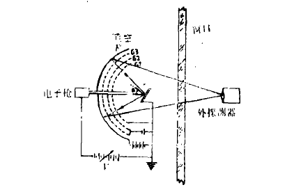
图1 原理图
改变入射电子能量,根据布喇格条件,衍射亮斑随之在荧光屏上移动,且每个亮斑的衍射强度连续变化。可在观察窗外面用光度计、摄象采集系统或照相办法,测量不同衍射束强度的1-V或1-E (E为电子能量)曲线,又称LEED强度谱,进行LEED定量分析用。如测量每个亮斑的角分布,可研究不完整表面的特性。LEED分析器的另一种形式是在球形栅网前加法拉第杯,测量背射电子强度。法拉第杯由机械或步进控制在各方位上移动。它的接收灵敏度高,但操作不方便,速度慢。第三种形式是将隧道倍增管阵列板和电阻板,或其它形式的摄象增强接收系统装在超高真空室中,直接测量衍射束强度.也可用示波器或投影荧光屏做外显示[4]。
3.应用
3.1用低能电子衍射研究GaAs(110)表面的弛豫
GaAs晶体是属于化合物半导体,As和Ga 原子间都是采用sp3杂化轨道相联结的极性共价键. 它的(001),(111)是极性表面, 原子晶体表面的特征显著, 表面上有大量悬挂键, 重构现象普遍. 但(110)是非极性表面, 离子晶体表面的特征显著, 表面悬挂键基本消失, 至今未发现重构现象。但此表面总是弛豫的。
关于(110)表面的弛豫已有大量研究工作。 但随作者采用的方法和模型不同, 所提出的此表面结构参数彼此差别较大。
研究使用低能电子衍射研究了GaAs(110)表面的弛豫[5]。发现当理论与实验之间符合得最好时,得到的结构是,保持表面上As-Ga键长不变用一个27.32°士0.24°的旋转角(ω),使As原子向外移动0.10±0.02Å,Ga原子向内移动0.55±0.02Å,而从Ga到第二层时空间为d1=1.45±0.01Å,从第二层Ga到第三层的空间为d2=2.01±0.01Å。对此结构As的背键长lAs= 2.43±0.01Å(收缩0.56%},而Ga的背键长lGa= 2.253±0.004Å(收缩8.0%)。
3.2用低能电子衍射研究小面结构
在某些晶体表面上,会出现与该表面晶格取向不同的其它晶面,它们可能是晶体表面上台阶的断面,也可能是在晶格表面上出现的一些小丘、平台、锥体或各种类型凹坑的边界面,这些在表面上出现的取向与表面相异的晶面统称为“小面”[6]。
确定这类小面的结构,即它们的晶格取向和周期性,有着特殊的意义。众所周知,晶体表面特有的电子性质和它的晶格结构往往密切相联系着[7],小面的存在有可能影响或根本改变原来晶体表面的电子性质。另外,这类小面的出现有各种不同原因,或者决定于晶体本身的固有特性,或者来源于制备表面的各种处理手段。了解了这类小面的结构,就为进一步探讨上述问题打下基础。
低能电子衍射(LEED)是研究晶体表面结构的主要手段.当表面上形成的小面是有序时,这些小面所对应的LEED图样将呈现特殊的行为,利用这一点就有可能确定小面的晶向和周期性。
3.3用低能电子衍射研究固体表面的原子排列
研究固体清洁和吸附表面的原子排列,是了解固体表面结构和性质的基础。只有对固体表面二维晶格的周期性(即原胞)、原胞的组成与各原子的排布、原胞与衬底之间的距离等确定后,才能比较全面地阐明表面的物理和化学性质以及表面与原子或分子的相互作用[8]。
LEED谱用于确定表面原胞组成和原子在原胞中的位置以及表面原胞与衬底间距等参数,因此它是表面结构的特征谱。只要用精确可靠的实验方法获得5-6条LEED谱后,就以此为标准,选用合理模型和参数,并不断调整表面原子位置使理论计算与实验结果一致,这样就可确定表面结构。
用LEED研究清洁和吸附固体表面的原子结构已近800个。从文献可知,已研究过的大多数清洁的金属固体表面与衬底相同,且稳定。但一般只研究了一个晶面,只有Ni, Al和Fe三个晶面都研究过了。从结果看来Ni, Al和Mo虽然表面原胞与衬底的相同,但在垂直于表面的方向上原子间距有膨胀和收缩现象,并随晶体种类和晶面不同,膨胀和收缩的程度也不同。这是否具有特定的规律,有待今后证实。
在原子晶体各晶面和5d过渡金属的(100)面上,普遍存在重构现象。这是由于此类晶面上存在大量悬挂键之故。这些悬挂键好象半电场,处于此种场中的原子不稳定,故可重排成稳定的结构。
在离子晶体表面上的正、负离子有向内、外移动几埃(Å)的现象。一般阴离子极化变形较大,被表面场极化后离子半径增大,故向外移动;而阳离子极化变形较小,故向内移动。因此离子晶体表面总是被负电荷所屏蔽。
4.结语
近10多年来虽然已对各种晶体表面进行了大量研究工作,其成果已在许多科学、科技和生产中发挥了很好的作用。但研究工作还限于部分晶面。可以预言随着对各类晶体、无定形体、有机体和生物体等表面全面深人了解后,它将在许多学科(如,材料、半导体、金属和超高真空等物理;腐蚀和催化等化学)和技术(如,固体器件、大规模、超大规模和光集成电路以及遥感技术等)领域中发挥更好的作用。
参考文献
[1]. C.Daeisson and L.Germer, Nature 119(1927)5589 Phys.Rev.,30(1927)705.
[2]. J.Maclaren, J.Pendry,P.Rous,D.Saldin, G.Sornorjai, M.Van Hove and D. Vvedensky. Surface Crystallo?raphic Information Service一A Handbook of Surface Structures. D.Reidel Publishing Company,1987.
[3]. 杨玉琨.低能电子衍射[J]. 物理实验,1983,3(2):88-91.
[4]. 伍乃娟.低能电子衍射[J]. 物理,1983,13(10):596-608.
[5]. 蓝田,徐飞岳.用低能电子衍射研究GaAs(110)表面的弛豫[J].物理学报,1989,38(3):357-365.
[6]. 陈平,侯晓远,丁训民,等.用低能电子衍射研究小面结构-在VIII族化合物半导体表面的应用[J]. 半导体学报,1986,7(1):65-72.
[7]. A.Kahn,Surface Sci. Reports,3,193(1983).
[8]. 徐飞岳.用低能电子衍射研究固体表面的原子排列[J]. 化学通报,1983,5:21-27.
第二篇:超低能电子衍射技术及应用实例
http://www.
Angular-resolved VLEED:
Bond geometry, Valence DOS, Brilliuon zones, Potential Barrier, Surface Charge Density, Atomic Valences and bonding kinetics
Chang Q SUN
Nanyang Technological University, Singapore 638075
ABSTRACT
It is shown that the very low energy electron diffraction (VLEED, at E = 6 - 12 eV), furnished with appropriate modelling approaches, is able to reveal comprehensive information about the details of a surface from the right top two atomic layers. Constructing Brillouin zones from the critical positions on the angular-resolved VLEED spectra yields information about valence bands and in-plane reconstruction of the O-Cu(001) surface. Decoding the fine-structure features with new models [Prog. Mater Sci. 48, 521 (32003)] rewards us with consistent understanding of the bond formation and its consequences. It is interpreted that the bond forming results in the dislocation of surface atoms, the variation of energy states, the nonuniformity and anisotropy of the potential barrier, and the reduction in both work function and inner potential of the surface. Therefore VLEED is promising technique for low dimensional systems.
- 1 -
http://www.
I INTRODUCTION
Very-LEED (VLEED) at energies covering valence bands has tremendous advantages though there appeared some difficulties in decoding the fine-structure features [1-5]. The measured data contain profounding information such as the crystal geometry, potential barrier and energy states of a surface. However, much patience and sophisticated effort is strongly required to assimilate properly the knowledge [1,2]. Recently, a number of researchers [3-5] devoted their efforts to using VLEED to characterise the energy states above vacuum level of surfaces. Strocov et al [3,4] demonstrated that the VLEED measurements are ideally suited for accurate determination of the desired upper states. Knowledge about the excited states could be substantially improved than the band mapping by photoelectron spectroscopy [4]. Bartos et al
[5] found that corresponding theoretical I-V curves could be obtained in good agreement with experimental data from the Cu(111) surface when the anisotropy of the electron attenuation was taken into account. With new modelling approaches [6-8] and a multi-atom code [9], we have been able to classify the factors dominating the spectral features [8], and hence open the possibility of using VLEED to seek insight into the nature and the dynamics of the O-Cu(001) surface bonding [10]. VLEED technique is becoming increasingly significant and it is a potentially powerful tool in surface science [1-12]. The details about this technique and its capacity please refer to Refs. [1,2,7-11].
There are two characteristic features on the measured VLEED spectra. One is the sharp solitary peaks whose positions rely heavily on the crystal geometry and the incident and azimuthal angles of the incident beam [1,2,9], and the other is the fine-structure features coming from the interference between the measured beam and preemergent beams that reflect repeatedly between the substrate lattice and the electrical potential barrier of the surface (SPB)
[1,2,9,11,12].
The sharp peaks converge into the thresholds of emerging new beams inside the crystal, as found by many researchers from the O-Ru [2], Cu(111), Ni(111) [3] and the ZnO(0001) [13]. These features are suggested as being issued from the energy-band structure [1-4,13]. The troughs relate to the intensity variation caused by the wave-like energy dependence of the additional sextets in VLEED pattern [14]. The relationship between the band structure and the elastic reflection coefficient can be obtained through the matching method [15-17]. In this approach the elastic reflection coefficient is determined by matching the vacuum wave-function with the superposition of Bloch waves excited in the solid. It is expected [18,19] that the energy location of a trough in the spectrum, corresponding to the rapid change of reflection, coincides with the location of the band-structure critical positions in the Brillouin zone (BZ). Therefore, it is possible, as realised by Jaklevic and Davis [14], to determine the connection between the VLEED profile and the band structure by directly measuring the positions of the critical points. The critical positions to be further concerned are hence very important to the VLEED studies.
The conjunction of the SPB with the multiple scattering gives rise to the interesting phenomena of surface states, surface resonances and VLEED fine structures [12]. Occupied surface states and resonances are of great importance in determining properties of surfaces [1,12]. The VLEED fine-structure features relate to the electronic structure that varies with atomic positions and atomic states. Unlike the normal LEED in which interactions with ion cores predominate, the VLEED data are very complicate as the VLEED integrates the effects of: (1) diffraction by the crystal geometry, (2) interference by the SPB and, (3) attenuation by the energy exchange with surface electrons [8-10]. Therefore, it appeared impossible to decode the VLEED data precisely as the decoding involves so many correlated factors.
In convention, it is often to employ a known crystal structure and then to feature the SPB. Typical methods have been demonstrated in Ref. [9] in which we treated all the parameters required in calculations completely independent, such as atomic dislocations and the uniform-SPB. The elastic potential was presumed as a uniform layer of interference, and the inelastic potential was simplified as monotonic energy dependence. The uniform-SPB - 2 -
http://www.
approximation is good enough to describe a nearly-ideal Fermi system such as clean metal surfaces which exhibit small ion-core corrugations and uniform energy states, as revealed by STM and STS [20,21]. The uniform-SPB approximation, however, performs not satisfactorily in the O-chemisorbed surfaces, as it was demonstrated in Refs. [9,10]. Particularly, agreement between the calculated and measured O-Cu(001) spectra near the <11> direction was inaccessible though various structure models and SPB-parameter values were considered [6,9]. Even though spectra at azimuths far away from the <11> direction looked fit, the spectral shape-similarity was offset by varying the values of the parameters from azimuth to azimuth. Besides, the independent treatment of the correlated parameters leads to infinity in mathematical solutions that should be certain in reality and sensible in physics [7,8]. Difficulties in convention wisdom
[6,8,9] challenge further effort in improving the decoding method and re-evaluating the capacity and reliability of the VLEED technique.
The purpose of this work is to show that the VLEED possesses the capacity of simultaneously determining all the categories that contribute to the reflection. First, we deal with the critical positions on the O-Cu(001) VLEED spectra, in particular, the correlation among the critical positions, in-plane reconstruction and valence bands. Then we decode the spectra with a multi-atom code and new modelling approaches. The decoding improves our understanding of the bond formation and its consequences. It becomes certain that the bonding results in the variations in features as characterised by crystallography, spectroscopy and microscopy, as well as the reduction in work function and inner potential. The full capacity of the VLEED technique can thus be uncovered with appropriate modelling approximations and decoding methods.
II VLEED DATA, CODE, and MODELS
2.1 Angular-resolved VLEED spectra
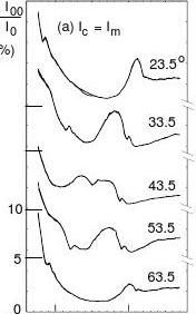
The VLEED (00) beam I-V profiles reported by Hitchen and Thurgate [22], as shown in Fig. 1, is the complete angular-resolved set available to date. These spectra to be decoded were collected from a 300 L oxygen-exposed Cu(001) surface. For the symmetry consideration, angles from 18.5° to 63.5° with 5° increment are sufficient to represent the full azimuth of the surface. The incident and azimuthal angles of the electron beams are illustrated in Fig. 2(a). A detailed description of the apparatus and techniques for data acquisition was given by Hitchen et al [23]. The features of the measured VLEED profiles in Fig. 1 can be summarised as follows:
(1) Two sharp, solitary troughs or violent peaks (indicated by dotted lines) appear on each
curve. These two troughs move away from each other as the azimuth moves away from the <11> direction. The two angular-dependent sharp features divide the VLEED energies (6.0 ~16.0 eV) into three regions. Calibration of these critical positions gave the reduction in work function of 1.1 eV [22].
(2) The fine-structure feature (indicated by the dashed lines) splits into its separate components
as the azimuth moves away from the symmetric point 45.0°. The first component vanishes outside the region of 33.5° ~ 58.5°. The second one becomes narrower while moving away from the symmetric point. Further, the intensity of the second peak tends to be weaker when the azimuth is greater than 45.0°.
(3) The peak positions and intensities of the curves show a reduction in symmetry relative to
the symmetric centre. The reduction of the intensities at higher azimuth may come from the development of the reaction, as it was noted [24] that the long-term ageing leads to a general attenuation of the spectral intensity.
- 3 -
http://www.
2.2 VLEED multi -atom code
The multi-atom code was developed by Thurgate and Sun [9] from Van Hove and Tong's LEED package [25]. A full description of the multiple diffraction model and the calculation code is the subject of Ref. [9]. Excellent agreement of the VLEED data measured from the clean Cu(001) surface evidenced sufficiently that the code works well and the diffraction model is complete and correct [9]. The significance of the code lies in that:
(1) The SPB is treated as an additional interference layer adding to the crystal diffraction.
(2) Instead of the previous double-diffraction model proposed by Dietz et al [26], the
multiple-diffraction along the (00) beam direction is taken into account.
(3) This code suites for large complex unit meshes or adsorbed surfaces with multiple atoms,
for example, the Cu(001)-(√2×2√2)R45°-O unit cell contains four coppers and two oxygen adsorbates.
(4) During diffraction, partial of the (00) beam is diffracted into other directions. Having been
attenuated by the multiple random-diffraction, a fraction of such diffracted beams may converge back into the (00) beam. Such convergence occurs when the interference conditions are satisfied. i.e., coincidence in direction, phase-change and amplitude. The contribution of such kind multiple-diffraction is assumed insignificant to be neglected. This approximation is reasonable enough as at very low energies the contribution of high-order diffraction is negligible, as noted by Pfnür et al [2].
2.3 Models
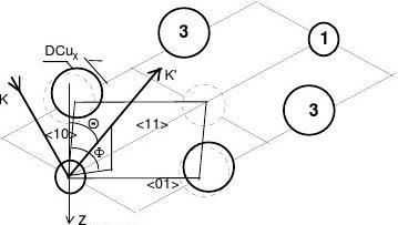
(1) In-plane primary unit cell
Fig. 2(a) shows a complex-unit-cell of the missing-row structure without adsorbate, which contains the in-plane primary-unit-cell that is the concern of the community of solid state physics. As it is known [27,28], the presence of defects and impurities, such as the missing-row vacancy and the oxygen adsorbate, has no effect on constructing either the real or the reciprocal lattice. Displacements of lattice atoms, such as the DCux for the atoms closing to the missing-row, however, distort both of the lattices.
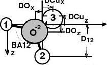
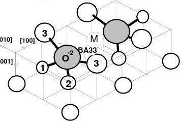
(2) Cu3O2 bonding
The bond model developed recently [6] for the Cu(001)-(√2×2√2)R45°-O phase is shown in Fig. 2(b) and summarised as follows. The Cu3O2 structure comprises two quasi-tetrahedral Cu2O units (12O33). The O-2 hybridises and interacts with the Cu(001) surface through two Goldschmidt-contraction ionic bonds (1-O-2 and 2-O-2) and two nonbonding lone pairs of electrons (3-O-2) [29-31]. The atom labelled 1 is Cu+2, atom 2 is Cu+ and atom 3 the lone-pair-induced Cu dipole with expansion in size and elevation of energy states. M is the missing-row vacancy. This model represents that the "two O-2 get four electrons from three coppers"[32], which can be formulated as:
O2(adsorbate) + 4 Cu(surface) + 2 Cu(substrate)
? 2 O-2(hybrid) + 2 Cu+(substrate) + Cu+2(surface) ..................... (Cu3O2 bonding)
+ 2 Cu(buckled dipole) + Cu(missing-row vacancy) .................. (effects of bonding)
(2.3.1)
The bond variables of a Cu2O structure are the effective contracting factors Q1 and Q2 for - 4 -
http://www.
bond length [BLi = (1.32 + 0.53) × (1 - Qi) ?, i = 1, 2], the bond angle BA12 (∠1O2) and the lateral displacement of the Cu dipole DCux. All the five atomic-shift parameters (layer spacing D12 and atomic shifts DOx, DOz, DCux, DCuz) required in VLEED calculations are given by BA12, DCux if the effective coordination numbers of the 1-O-2 and the 2-O-2 are assumed as 4 and 6. The bond variables are limited within the parameter space:
{BA12 ≤ 104.5° [29]; DCux ≈ 0.25 ? [6, 33,34]; (Q1 = 0.12, Q2 = 0.04) [31]}
? (D12, DOx, DOz, DCux, DCuz)
(3) Single-variable parameterised nonuniform SPB
As a result of the Cu3O2 bonding (Eq. 2.3.1), the missing-row vacancy and the buckled dipole localise the surface electrons, as observed with STM by Jensen et al [20]. The strong localisation leads to the nonuniformity in the SPB.
The elastic potential, ReV(z), is expressed with the model formulated by Jones, Jennings and Jepsen [35], as shown in Fig. 3. The z - axis directs into the crystal. V0 is the muffin-tin inner potential constant of the crystal and z0, the origin of the image potential. The degree of saturation is described by the λ parameter. One important fact is that the ReV(z) changes its form at z = z0 from the pseudo-Fermi-z function to the 1/(z-z0)-type image-potential. The ReV(z) satisfies the Poission's equation ?2[ReV(z)] = -ρ(z) [36], and hence ?2[ReV(z0)] = -ρ(z0) = 0
[7-9]. This relation limits the surface electrons to occupy the region within z0 - the origin of the image-plane.
The spatial variation and the energy dependence of the inelastic potential ImV(z, E) is modelled as [7-9]:
ImV(z, E) = ImV(z) × ImV(E)
- φL)/δ] = γ × ρ(z) × exp[(E
γ×exp[
=E?φL(E)
1+exp(?
(2.3.2)
where γ and δ are constants determined by the intensity of damping, and they can be used to compensate for the accuracy of the calibration of spectral intensity [8]. The ρ(z) describes the electronic distribution with a Fermi-z function [7-10]. The z-directional integration of the ρ(z) yields the local density-of-state (DOS) n(x, y). Since the VLEED integrates over large surface area, all the quantities depending on coordinate (x, y) become E dependants. For instance, at a certain energy the VLEED integration changes the n(x, y) into n(E) that relates to the occupied DOS. The DOS contributes to the ImV(E) through the work function φL = E0 - Ef[n(E)]2/3 [37], where the E0 and Ef are the vacuum level and the Fermi energy of clean surface. The ImV(z, E) represents that the single electron-excitation dominates at energies below plasma-excitation, and this process occurs in the electron occupied space with any energy greater than work function
[1,38].
In order to reduce numerical efforts and represent the correlation among the parameters, all the parameters in the ReV(z) and ImV(z, E) are defined as functional-dependant on the character z0:
- 5 -10)α(z0) ]
http://www.
λ(z0) = λ0M[x + (1 - x) × exp[?(z1(z0) = z0exp[?(z0?z0Mz0?z0Mλz)2], (2.3.3) τ1)2], (2.3.4) α(z0) = 1/λ(z0)×exp[?(z0?z0m
τ2)2], (2.3.5)
where the constants λz = 0.8965, x = 0.4732 are obtained with a least-square analysis of the calculation results. λ0M = 1.275 corresponds to z0M = -3.425 (atomic unit). The z0m = -1.75 (a.u.), τ1 = 0.75 and τ2 = 1.50. These constants were optimised against the criteria [7,8], i.e., to ensure the uniqueness in z0(E) and to minimise the ?z0 in solutions (as denoted in Fig. 6).
The functional forms of (2.3.4-6) represent that in the dipole region the electronic cloud shifts outward and becomes denser while in the missing-row site the vacancy is not occupied due to the absence of freely moving electrons in the strongly localised system [6].
Fig. 3 (a) shows the forms of ReV(z), ImV(z) and their correlations. Fig. 3(b) shows the z0 dependence of other parameters. If z0 is constant the nonuniform-SPB approximation will degrade into the convention uniform. The validity of such an approximation has been demonstrated in Refs. [7-10].
III ANALYSIS & DISCUSSION
3.1 Critical positions
(1) Brillouin zones and effective masses of electrons
It is realised [1-5,9,13-18] that the emergence of new diffraction beam is independent of the inner potential and the barrier shapes. It depends only on the incident diffraction conditions and the two-dimensional geometry of the surface. The emergence happens when the lateral components of the diffracted k'// and the incident k// satisfy the Bragg diffraction formula,
(3.1.1) k'// - k// = g,
where g is the reciprocal lattice vector. It is the very Bragg condition that yields the band-gap reflection at the boundary of a BZ [27,28]. Therefore, the sharp features closing to the emergence of new beam on the VLEED spectra can be attributed to the band-gap reflections.
Accordingly, two-dimensional BZs can be constructed from the sharp-peak positions in Fig. 1, and the corresponding energies in Table 1. The location of a peak Ep can be decomposed in k-space as (in atomic units: m = e = h = 1, 1 a.u. = 0.529 ?, 27.21 eV):
222[k<01>+k<10>+kz]Ep= 2m*
**with k<10>=2mEpsinθcosφ, and k<01>=2mEpsinθsinφ, (3.1.2)
where m*, the effective mass of electron, is introduced to compensate for the reduction of the diffracted k' due to its energy loss. θ and φ represent the incident and azimuth angles of the incident beam. The resultant of the wave vectors, k<10> and k<01>, extends from the centre to the boundary of the BZ. The first two experimental BZs then can be drawn by optimising m* to match the theory calibrations (k<10> = k<01> = nπ/a, n = 1, 2) [28] as shown by the solid lines in Fig. 3. The effective masses of electrons surrounding BZ boundaries are optimised with least-square method. The optimal values, m*1 = 1.10, and m*2 = 1.14, coincide with the energy-loss of the diffracted beam (k' = k/m*1/2) that increases with the kinetic energy [39]. It - 6 -
http://www.
is noticed that the first BZ contracts at Y while the first BZ expands near X. The contraction at Y can be interpreted as resulting from the atomic shift along the <11> direction, while the expansion near X needs to be identified.
(2) In-plane reconstruction
The mutual-reciprocal relation between the k-space with basic vector kj and the r-space with ai
[27,28]:
ai ? kj = 2πδij;
if i = j, δij= 1, else δij = 0, (3.1.3)
implies that the deviation of the experimental BZ from the ideal form originates from the deformation of the primary unit cell. Hence, one may trace inversely the DCux from the contraction of the BZ at Y. The ΓY (= 1?ki + kj?= √2π/a, [27,28]) corresponds to a quantity a<11> through the 2
reciprocal relation (3):
(3.1.4) a<11> ? (ki + kj) = a<11> ? 2ΓY = 2π,
which yields
a<11> = π/ΓY = a/√2,
corresponding to the shortest row spacing on the (001) surface (Fig. 2). Taking the logarithm and derivate from both sides of Eq. (3.1.4), we have
da<11>dΓY+=0. a<11>ΓY
Thus, the lateral-atomic shift can be expressed as:
DCux = da<11>
*a<11>a2=?dΓY=?dΓY. (3.1.5) 2πΓY
*1.10, θ = 69.0° and Ep1 = 10.4 eV = 0.3804 a.u.(at 43.5° close to the <11> Substituting m1 = direction) into Eq. (3.1.2) yields ΓY' =2m1Ep1sinθ = 0.8104 (1/a.u.). On the other hand,
by adopting a = 2.555/0.529 = 4.8308 (a.u.), we can have the theory value ΓY = √2π/a = 0.9217 (1/a.u.). Therefore,
a2
(ΓY' - ΓY) DCux = - 2π
= 0.4133 a.u. ? 0.22 ?, (3.1.6)
which coincides with the values (0.2 ~ 0.3 ?) optimised with LEED [33], XRD [34] and VLEED (~ 0.25 ?) as shown in Section 3.2. The accuracy of this estimation is subject to the measured Ep1.
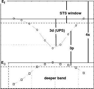
(3) Valence bands
It has been identified in this work that the critical positions correspond to the boundaries of the BZs which divide the VLEED energies into three regions (see Fig. 1). These different regions can be classified as the valence bands as denoted in Fig. 4. The variations of the band-width with the azimuth agree with what was noted for example by Kittel [27] and Omar [28] in classical text books. The energies of the current VLEED (6.0 ~ 16.0 eV) cover part of the windows of the STS (~ 5.0 ± 2.5 eV) [21] and the UPS (10 ~ 50 eV) [40]. The first sharp-peak positions varying from 7.0 to 10.4 eV can be ascribed as the bottom of the 3d band, which agrees with the known 3d band structure, 2.0 ~ 5.0 eV below Ef (5.0 eV), as detected by - 7 -
http://www.
Angular-resolved UPS [41]. Accordingly, the region between the two sharp peaks corresponds to the 3p band. The 3p band overlaps partially the 3d due to the azimuthal effect. The 4s band between Fermi energy Ef and vacuum level E0 (12.04 eV) [37] fully covers both 3p and 3d. Energies higher than the second BZ correspond to deeper bands that need to be classified.
3.2 Fine-structure features
The calculations were conducted by assuming that the crystal structure was unchanged during the data acquisition. In fact, the specimen ageing influences slightly on the spectra by modifying the energy states below 7.5 eV and the geometry DCux [10]. The calculation procedures are summarised as follows. First, referring to the value of the z0 for clean Cu(001) surface which is in the range from Jellium edge to atomic radius (1.8 ~ 2.5 Bohr Radii) [9,23], we let the calculation code scan z0 over -2.5 [23] ± 1.0 Bohr radii, with step of δz0 = 0.25 Bohr radii to search possible solutions. The output of the z0-scanning calculation is the contour of z0-E. This plot also assists us to optimise the constants (such as γ, δ, τ1, τ2) involved in the SPB functions (2.3.3-5). Then, after all the constants are fixed, the calculation code automatically optimises z0(E), (with step of δz0 = 0.25 ~ 0.0001 depending on the value of Ic/Im) to match (with ± 3% error) calculated Ic with measured Im at each energy. Besides the bond geometry and the inner potential, the outcome of the z0-optimising calculation is eventually the duplication of the measured Im and the corresponding energy dependence of z0(E).
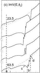
The matching between calculated and measured spectra for all the ten azimuthal angles has been obtained but for comparison purpose we just show the five replicas in FIG 6(a). Corresponding energy-dependence of the optimised z0(E) and the inelastic damping ImV(E, φL) are shown in panels (b) and (c). As references, the constant z0 (-2.5 a.u.) for Cu(001) [23] and the monotonic ImV(E, 5.0) in dotted lines are compared. Information available from the decoding is summarised in Table 2. All the results agreeing with previous observations can be understood as the effect of the bond formation.
(1) Bond geometry-crystallography
Atomic dislocations, layer-spacing relaxation and in-plane reconstruction as well as the adsorbate position are given by the bond geometry [6,8]. The atomic arrangement agrees with the conclusion drawn from the effective-medium theory calculations by N?rskov et al [42], and it was understood that the oxygen atoms go underneath the first layer for bonding. Meanwhile, there is a pairing of the Cu atoms (dipoles) crossing over the missing row. The relaxation is determined by the bonding between the adsorbate and the substrate as noted by Van Hove and Somorjai [43]. From the perspective of bond forming, absolute accuracy in static atomic position seems to be less sensible, and therefore, discrepancies in atomic positions should be allowed.
(2) Reduction in the inner potential and work function
As it can be seen from Fig. 3(b), the work function reduces its value with the outward shift of the z0. This reduction originates from the formation of the surface dipole layer, as noted previously by Ertl and Rhodin [44]. Current model explicates that the dipole layer is induced by the nonbonding states of the hybridised-O-2. The amount of the reduction is about 1.20 eV (denoted in Fig. 3(b)) which coincides with the value (~ 1.2 eV) detected from the O-Pt surface by Rotermund et al [45]. The reduction in work function may also provide an understanding of the STS observations by Chua et al [21] from the O-Cu(110) showing the occupation of the - 8 -
http://www.
surface states (0.8 ~ 1.8 eV above Fermi level) by the polarised metal electrons [6].
The oxygen adsorbate reduces the muffin-tin inner potential V0 from 11.56 of Cu(001)
[9,23] to 10.50 eV, (9.2% reduction). It is found in Ref. [9] that the reduction depends on the structure models employed. For a c(2×2)-O [34] and a (2√2×√2)R45°-O [33] superstructure the reduction is 1.21 and 2.15 eV, respectively. Similar conclusion has also been made by Pfnür et al
[2] who found in their VLEED calculations it necessary to use a step function to describe the reduction of the inner potential of the top layer of O-Ru surfaces. However, with few interpretations the underlying mechanism of the O-reduced inner potential in VLEED remains ambiguous [2,9].
We may attribute the reduction in V0 to the bond formation as discussed below. From a classical point of view, the total number of electrons contributing to the inner potential will be reduced for the chemisorption of the O2 (with 8 electrons for each O atom) and the removal of one Cu (with each Cu atom there are 29 electrons). Initially, there are four Cu atoms in a complex unit cell as shown in FIG. 3(b) [8,9]. During the reaction the nuclei charge of Cu is unchanged. The oxygen atoms catch two electrons from the substrate, which also contributes to the variation of the inner potential of both the top and the second layers. Hence, the relative variation of the electron number in the top layer is:
{[29e × (4 - 1)] + [8e × 2 + 2e]}/(29e × 4)
= 105/116
= 90.5% (9.5% reduction),
which coincides with the VLEED optimisation (9.2%) with the current bond configuration. Therefore, the reduction in both the work function and the inner potential results from the surface-bond forming.
(3) Joint features of microscopy and spectroscopy
As mentioned before, the z0(E) curves in Fig. 6(b) exhibit the joint features of topography and spectroscopy. It is noticed that the shapes and the intensities of z0(E) curves, as well as the damping in Fig. 6(c), vary apparently with the azimuth. At 43.5°, closing to the <11> direction, the z0(E) curve provides the maximal ?z0 ~ 0.52 ? closing to the scale difference of the STM image [20]. This can be clear indication of the nonuniformity and anisotropy of the SPB, as noticed by Baribeau et al [15] in their VLEED simulations that the damping is no more isotropic due to oxygen adsorption. It is clear now why we could not fit the VLEED spectra near the
<11> direction without considering the anisotropy and nonuniformity of the SPB [6,9].
The calculations provide a preliminary understanding of the energy states that contribute to the damping. As indicated in FIG. 6(b, c), there are several notable regions showing DOS features:
(a) Features below 7.5 eV are independent of the azimuth. These humps coincide with the
STS observations by Chua et al [21] and these features have been interpreted as the contribution of the nonbonding states of the hybridised-O-2 [6,8] which is absent from the very low oxygen exposures (≤ 25 L) [10]. The coincidence of the VLEED with the STS in the above-Ef (polarisation states or reduction in work function) and the below-Ef (hybridisation sates) features can be convincing evidence that the oxygen adsorbate hybridises itself and polarises electrons of its neighbour metal atoms [6].
(b) The band-gap reflection along the boundary of the second BZ is apparent, while such kind
of reflection is invisible near the symmetry point (45°) at the boundary of the first BZ. The invisible features are obviously due to the overlap of the 4s3d3p bands (see Fig. 5).
(c,d) The damping surrounding the second BZ may be featured as the electron excitation at the
edges of different bands. The excitation of electrons from the bottom of a band seems to be harder than that from the top edge of a band where the electrons are denser.
- 9 -
http://www.
IV SUMMARY
We have thus presented ways of extracting information from the measured data and uncovering the full capacity of the angular-resolved VLEED. It is suggested that the complete concept of VLEED technique should contain the high-resolution data, calculation codes, modelling approaches and decoding methods as well. The comprehensive knowledge obtained with the VLEED can be summarised as follows:
??BZs?Energy bands + Reconstruction??Crystallography????Adsorbate position +Atomic dislocations+ Relaxation????Microscopy: Local DOS:ρ(x,y,z)?ReV(z), ImV(z)???Bond model??SPB [z0(E)]???Spectroscopy: DOS:n(E)?Work function ?ImV(E)?????Muffin-tin inner potential constant V0???
The consistent understanding of the O-Cu(001) surface reaction and the coincidence in the observations with other techniques such as the STM/S can be further evidence that the VLEED is reliable and powerful in revealing information of surface processes, and the corresponding code and modelling approaches are substantially realistic and complete, as demonstrated in recent publications [6-10].
V ACKNOWLEDGMENT
Beneficial discussions with P. Jennings, critical review by A. Stelbovics, M. Donath, S. Tear and G. Russell and kindly providing the VLEED data by G. Hitchen and S. Thurgate are all gratefully acknowledged.
References
[1] R.O. Jones and P.J. Jennings, Surf. Sci. Rep. 9, 165 (1988).
[2] M. Lindroos, H. Pfnür and D. Menzel, Phys. Rev. B33, 6684 (1986); H. Pfnür, M.
Lindroos and D. Menzel, Surf. Sci. 248, 1 (1991).
[3] V.N. Strocov, Inter. J. Mod. Phys. B9, 1755 (1995) (reference therein).
[4] V.N. Strocov, H.I. Starnberg and P.O. Nilsson, J. Phys. C8, 7539 (1996); V.N. Strocov,
H.I. Strarnberg, P.O. Nilsson and L.J. Holleboom, J. Phys. C8, 7549 (1996); V.N. Strocov and H.I. Starnberg, Phys. Rev. B52, 8759 (1995).
[5] I. Bartos, M. A.Van Hove and M.S. Altman, Surf. Sci. 352, 660 (1996); I. Bartos, P.
Jaros, A. Barbieri, M.A.Van Hove and W.F. Chung, Q. Cai and M.S. Altman, Surf. Rev. & Lett. 2, 477 (1995).
[6] S.M. Thurgate and C.Q. Sun, Phys. Rev. B51, 2410 (1995).
[7]-[10] C. Q> Sun, Prog. Mater. Sci. 48, 521-685 (2003)
[11] E.G. McRae, Rev. Mod. Phys. 51, 541 (1979).
[12] M.A. Van Hove, W.H. Weinberg and C.-M. Chan, Low-energy Electron Diffraction:
Experiment, Theory and Surface Structural Determination. Springer-Verlag Berlin, - 10 -
http://www.
1986.
[13] P.J. M?ller, S.A. Komolov and E.F. Laznev, Surf. Sci. 307/308, 1177 (1994).
[14] I. Bartos and J. Koukal, Surf. Sci. 251/252, 508 (1991).
[15] J.M. Baribeau, J. Lopez and J.C. Le Bosse, J. Phys. C18, 3083 (1985).
[16] R.C. Jacklevic, L.C. Davis, Phys. Rev. B26, 5391 (1982).
[17] E. Tamura, R. Feder, J. Krewer, R.E. Kirby, E. Kisker, E.L.Garwin and F.K. King,
Solid State Comm. 55, 543 (1985).
[18] S.A. Komolov, Total Current Spectroscopy of Surfaces, Gordon and Breach, New York,
1992.
[19] H.-J. Herlt, R. Feder, G. Meister and E. Bauer, Solid State Comm. 38, 973 (1981).
[20] F. Jensen, F. Besenbacher, E. Lagsgaard and I. Stensgaard, Phys. Rev. B42, 9206
(1990).
[21] F.M. Chua, Y. Kuk and P.J. Silverman, Phys. Rev. Lett. 63, 386 (1989).
[22] G.J. Hitchen and S.M. Thurgate, Phys. Rev. B38, 8668 (1988).
[23] G.J. Hitchen, S.M. Thurgate and P.J. Jennings, Phys. Rev. B44, 3939 (1991).
[24] G.J. Hitchen, S.M. Thurgate and P.J. Jennings, Aust. J. Phys. 43, 519 (1990).
[25] M.A. Van Hove and S.Y. Tong, Surface Crystallography by LEED, Springer, Berlin,
1979.
[26] R.E. Dietz, E.G. McRae and R.L. Campbell, Phys. Rev. Lett. 45, 1280 (1980).
[27] C. Kittel, Introduction to Solid State physics, 5th ed., Wiley, New York, 1976.
[28] M.A. Omar, Elementary Solid State Physics: Principles and Applications,
Addison-Wesley, 1975.
[29] C.W. Keenan, D.C. Kleinfelter and J.H. Wood, General College Chemistry, P178, 6th
ed., Harper & Row Publishers, 1979. The oxygen hybridises and interacts with arbitrary element B to form the general OB2 tetrahedral structure through two bonding orbitals and two nonbonding lone pairs of electrons.
[30] L. Pauling, The Nature of Chemical Bond (Cornell University press 1939, 3rd ed., 1960).
The nature of a bond is determined by the difference in electronegativity between its components.
[31] V.M. Goldschmidt, Ber. Deut. Chem. Ges., 60, 1270 (1927). If an atom reduces its
CN from 12 to 8, 6 and 4, then its ionic radius will contract 3%, 4% and 12%.
[32] A.P. Cole, D.E. Root, P. Mukherjee, E.I. Soloman, T.D.P. Stack, Science 273, 1848
(1996).
[33] H.C. Zeng and K.A.R. Mitchell, Surf. Sci. 239, L571 (1990).
[34] T. Lederer, D. Arvanitis, G. Comelli, L. Troger and K. Baberschke, Phys. Rev. B48,
15390 (1993).
[35] R.O. Jones, P.J. Jennings and O. Jepsen, Phys. Rev. B29, 6474 (1984).
[36] P. Jennings, private communication, 1994.
[37] A. Beiser, Perspective of Modern Physics, 8th ed., McGRAW-HILL, Singapore, 1988.
[38] J.B. Pendry, Low Energy Electron Diffraction: The theory and its application to the
determination of surface structure, Academic press, London, 1974.
[39] E.G. McRae and C. W. Caldwell, Surf. Sci. 57, 766 (1976).
[40] D. Briggs, Handbook of X-Ray and Ultraviolet Photoelectron Spectroscopy, Heyden &
Son Ltd., 1977.
[41] R.A. Didio, D.M. Zehner and E.W. Plummer, J. Vac. Sci. Technol. A2, 852 (1984).
[42] F. Besenbacher and J.K. N?rskov, Prog. Surf. Sci. 44, 5 (1993); K.W. Jacobsen and J.K.
N?rskov, Phys. Rev. Lett. 65, 1788 (1990).
[43] M.A. Van Hove and G.A. Somorjai, Surf. Sci. 299/300, 478 (1994).
[44] G. Ertl and T.N. Rhodin, The Nature of Surface Chemical Bond, Amsterdam
North-Holland, 1979.
- 11 -
http://www.
[45] H.H. Rotermund, Surf. Sci. 283, 87 (1993); H. H. Rotermund, J. Lauterbach and G.
Hass, Appl. Phys. A57, 507 (1993); J. Lauterbach, K. Asakura and H. H. Rotermund, Surf. Sci. 311, 322 (1994).
Fig. Captions
Fig. 1. Angular-resolved VLEED profiles collected from the O-Cu(001) surface at 69.0°
incidence [22]. The azimuth angles are labelled for each curve. There is a "cross-point" at about 45° azimuth. Two small sharp peaks (indicated by dotted lines) appear on each curve. The broaden fine-structure feature (dashed lines) splits when the azimuth moves away from the <11> direction.
Fig. 2 Cu3O2 bond model for the O-Cu(001) surface [6,10] with illustration of the incidence
and azimuth angles. A complex unit cell containing the primary unit cell is shown in (a). The presence of defects such as the O adsorbate and the missing-row vacancy has no effect on the primary unit cell. However, the displacements DCux of the atoms closing to the missing-row will deform the lattice.
Fig. 3 Model of single-variable parameterised surface potential barrier. Panel (a) shows the
ReV(z) [35] and the spatial decay of the ImV(z, E) [7] and their correlation. Panel (b) shows the z0-dependence of all the SPB parameters, referring to Eqs. (2.3.3-5). E1 = 6.3 eV. The work function [37] reduces with the outward-shift of z0.
Fig. 4 The first two BZs, derived from the critical positions on the angular-resolved VLEED
profiles in Fig. 1 [22], are indicated by open circles and triangles, respectively. The theoretical BZs in soild lines are compared. Deformation of the first BZ can be seen in the diagram.
Fig. 5 Band structure extracted from the angular-resolved VLEED profiles [22]. The boundary
lines divide the VLEED energies into various bands as denoted.
Fig. 6 Outcomes of the single-variable parameterised calculations. (a) The matching of the
measured spectra and, (b) corresponding the z0(E) profiles. The maximal ?z0 at 43.5° can be evidence against constant solution for the O-chemisorbed surface. (c) The damping curve with four significant features. Regime <a> correspond to hybridised nonbonding states [6], <b> band gap reflection, <c> and <d> are the excitations occur at edges of different bands.
- 12 -
http://www.
Tables
Table 1 Positions of the sharp peaks, Ep1 and Ep2, in the angular-resolved VLEED profiles of the O-Cu(001) surface. The incident angle is kept constant at 69.0° [22]. Azimuth(°) Ep1(eV) Ep2(eV)
18.5 7.00 14.50
23.5 7.20 14.00
28.5 7.60 13.30
33.5 8.30 12.50
38.5 9.50 12.20
43.5 10.40
12.00
48.5 10.00
12.20
53.5 8.80 12.30
58.5 7.80 12.60
63.5 7.00 13.20
- 13 -
http://www.
Table 2. Summary of the information of the Cu(001)-(2√2×√2)R45°-O surface obtained from
the simulation of the angular-resolved VLEED spectra with new models [6-8].
Structural variation during the data acquisition is neglected.
Q1, Q2 0.12, 0.04 Controlling
[6,31]
102.0 [6,29] Bond BA12 (°)
DCux (?) 0.250 [6,34] Variables
Atomic
Shifts
(?) DCuz DOx DOz -0.1495 -0.1876 0.1682
D12 1.9343 Relaxation
Bond BA13 105.3
V0 10.50 Inner
potential (eV)
ImV(E) 0.9703 γ
6.4478 δ
Reduction of work 1.20 ?φ function (Fig. 3b) (eV)
Microscopy 0.52 ?zVLEED(?)
features
Spectroscopy < 7.5 eV Hybridisation
Band-gap
Boundary reflection
Band-edge
Boundary excitation
Velence bands Fig. 5
- 14 -
Angular-resolved VLEES of300 L O-exposed Cu(001)
Θ= 69.0o
18.5o
23.5
28.5
33.5
I00I038.5
43.5
48.5
53.5
58.5
63.5
7.510.012.515.0
Energy (eV)
- 15 -http://www. FIG. 1/Sun (arb. unit)
http://www.
x - 16 -
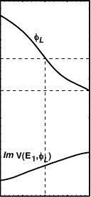
FIG.3(a,b)/Sun
http://www. VImV(z) = (z)ρImV(E)αz0z1?2[ReV(z)] = - (z)ρ1/λV0 27.511/λ6.00E (eV)4.5z(a.u.)3.0-21.5-40z (a.u.)0 - 17 -
http://www. 2
Y
FIG. 5/sun
1k (<01>π/a)0XΓ-1-2-1012k (<10>π/a) E (eV)5.010.0
15.015304560Azimuth ( )o - 18 -FIG. 4/Sun
http://www.
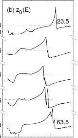
FIG. 6/Sun
7.512.5Energy (eV)- 19 -57.5
1