三、实验原理
浮点数的表达和计算是进行数字信号处理的基本知识;产生正弦信号是数字信号处理中经常用到的运算;C语言是现代数字信号处理表达的基础语言和通用语言。写实现程序时需要注意两点:(1)浮点数的范围及存储格式;(2)DSP的C语言与ANSI C语言的区别。
四、实验步骤
1. 打开CCS 并熟悉其界面;
2. 在CCS环境中打开本实验的工程(Example_base.pjt),编译并重建 .out 输出文件,然后通过仿真器把执行代码下载到DSP芯片中;
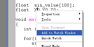
3. 把X0 , Y0 和Z0添加到Watch窗口中作为观察对象(选中变量名,单击鼠标右键,在弹出菜单中选择“Add Watch Window”命令);
4. 选择view->graph->time/frequency… 。 设置对话框中的参数: 其中“Start Address”设为“sin_value”,“Acquisition buffer size”和“Display Data size”都设为“100”,并且把“DSP Data Type”设为“32-bit floating point”,

设置好后观察信号序列的波形(sin函数,如图);

5. 单击运行;
6. 观察三个变量从初始化到运算结束整个过程中的变化;观察正弦波形从初始化到运算结束整个过程中的变化;
7. 修改输入序列的长度或初始值,重复上述过程。
五、实验心得体会
通过本次实验,加深了我对DSP的认识,使我对DSP实验的操作有了更进一步的理解。基本掌握了CCS实验环境的使用,并能够使用C语言进行简单的DSP程序设计。
从软件的安装到使用软件进行程序设计与仿真,锻炼了自己的动手能力,也遇到了不少的坎坷,例如芯片的选择,不能因为麻烦而省略该步骤,否则将会运行出错。
附录实验程序:
#include "math.h"
#include "stdio.h"
#define N 100
#define pi 3.14159
float sin_value[100];
float X0,Y0,Z0;
void main(void)
{
int i;
for(i=0;i<N;i++)
sin_value[i]=0;
X0=0.5; /* 0.100 0000 0000 0000 */
Y0=0.5; /* 0.100 0000 0000 0000 */
Z0=X0*Y0; /* 00.01 0000 0000 0000 0000 0000 0000 0000 */
for(i=0;i<N;i++)
sin_value[i]=100*(sin(2*pi*i/N));
}
龙 岩 学 院
实验报告
班 级 07电本(1)班 学号 2007050344姓 名 杨宝辉 同组人 独立
实验日期 20##-5-20 室温 大气压 成 绩
数码管控制实验
一、实验目的
1. 熟悉2812的指令系统;
2. 熟悉74HC573的使用方法。
3. 熟悉DSP的IO操作使用方法。
二、实验设备
1. 一台装有CCS2000软件的计算机;
2. 插上2812主控板的DSP实验箱;
3. DSP硬件仿真器。
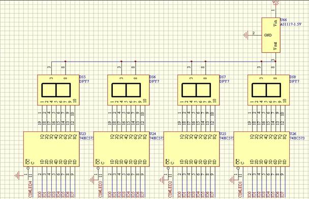
三、实验原理
此模块由数码管和四个锁存器组成 。数码管为共阴极型的。数据由2812模块的低八位输入,锁存器的控制信号由2812模块输出,但经由CPLD模块译码后再控制对应的八个
四、实验步骤
1. 把2812模块小板插到大板上;
2. 在CCS2000环境中打开本实验的工程编译Example_7segled.prj,生成输出文件,通过仿真器把执行代码下载到DSP芯片;
3. 运行程序;数码管会显示1~8的数字。
4. 参考源代码自行修改程序改变显示样式。
五、实验心得体会
通过本次实验中,基本掌握了2812的指令系统的特点,并能够了解并熟悉74HC573的使用方法,进一步加深了对DSP的认识。同时,通过实验操作DSP的IO操作使用方法,对于DSP的IO操作可以熟悉的运用,学到更多的知识。
程序见附录:
#include "include/DSP281x_Device.h" // DSP281x Headerfile Include File
#include "include/DSP281x_Examples.h" // DSP281x Examples Include File
// Prototype statements for functions found within this file.
void delay_loop(void);
void Gpio_select(void);
// Global variable for this example
short codetab[17]=
{0x4020,0x6cc0,0x5800,0x4840,0x6440,0xC040,0xC000,0x4cc0,
0x4000,0x4040,0x4400,0xE000,0xD080,0xE800,0xD000,0xD400,0xffff};
main()
{
short i;
// Step 1. Initialize System Control:
// PLL, WatchDog, enable Peripheral Clocks
// This example function is found in the DSP281x_SysCtrl.c file.
InitSysCtrl();
// Specific clock setting for this example:
EALLOW;
EDIS;
// Step 2. Initalize GPIO:
// This example function is found in the DSP281x_Gpio.c file and
// illustrates how to set the GPIO to it's default state.
// InitGpio(); // Skipped for this example
// For this example use the following configuration:
Gpio_select();
// Step 3. Clear all interrupts and initialize PIE vector table:
// Disable CPU interrupts
DINT;
// Initialize the PIE control registers to their default state.
// The default state is all PIE interrupts disabled and flags
// are cleared.
// This function is found in the DSP281x_PieCtrl.c file.
InitPieCtrl();
// Disable CPU interrupts and clear all CPU interrupt flags:
IER = 0x0000;
IFR = 0x0000;
// Initialize the PIE vector table with pointers to the shell Interrupt
// Service Routines (ISR).
// This will populate the entire table, even if the interrupt
// is not used in this example. This is useful for debug purposes.
// The shell ISR routines are found in DSP281x_DefaultIsr.c.
// This function is found in DSP281x_PieVect.c.
InitPieVectTable();
// Step 4. Initialize all the Device Peripherals:
// This function is found in DSP281x_InitPeripherals.c
// InitPeripherals(); // Not required for this example
InitXintf(); // For this example, init the Xintf
// Step 5. User specific code, enable interrupts:
GpioDataRegs.GPADAT.all=0;
Reg01=0x00;
GpioDataRegs.GPADAT.all=0;
Reg02=0x00;
GpioDataRegs.GPADAT.all=0;
Reg03=0x00;
GpioDataRegs.GPADAT.all=0;
Reg04=0x00;
while(1)
{
for(i=0;i<17;i++)
{
GpioDataRegs.GPADAT.all =~codetab[i];
Reg01=0x00;
delay_loop();
}
for(i=0;i<17;i++)
{
GpioDataRegs.GPADAT.all =~codetab[i];
Reg02=0x00;
delay_loop();
}
for(i=0;i<17;i++)
{
GpioDataRegs.GPADAT.all =~codetab[i];
Reg03=0x00;
delay_loop();
}
for(i=0;i<17;i++)
{
GpioDataRegs.GPADAT.all =~codetab[i];
Reg04=0x00;
delay_loop();
}
}
}
void delay_loop()
{
short i,j;
for (i = 0; i < 32767; i++)
{for (j = 0; j < 10; j++);}
}
void Gpio_select(void)
{ Uint16 var1;
Uint16 var2;
Uint16 var3;
var1= 0x0000; // sets GPIO Muxs as I/Os
var2= 0xFFFF; // sets GPIO DIR as outputs
var3= 0x0000; // sets the Input qualifier values
EALLOW;
GpioMuxRegs.GPAMUX.all=var1;
GpioMuxRegs.GPBMUX.all=var1;
GpioMuxRegs.GPDMUX.all=var1;
GpioMuxRegs.GPFMUX.all=var1;
GpioMuxRegs.GPEMUX.all=var1;
GpioMuxRegs.GPGMUX.all=var1;
GpioMuxRegs.GPADIR.all=var2; // GPIO PORTs as output
GpioMuxRegs.GPBDIR.all=var2; // GPIO DIR select GPIOs as output
GpioMuxRegs.GPDDIR.all=var2;
GpioMuxRegs.GPEDIR.all=var2;
GpioMuxRegs.GPFDIR.all=var2;
GpioMuxRegs.GPGDIR.all=var2;
GpioMuxRegs.GPAQUAL.all=var3; // Set GPIO input qualifier values
GpioMuxRegs.GPBQUAL.all=var3;
GpioMuxRegs.GPDQUAL.all=var3;
GpioMuxRegs.GPEQUAL.all=var3;
EDIS;
}
// No more.
交通灯控制实验
一、实验目的
1. 熟悉2812的指令系统;
2. 熟悉74HC573的使用方法。
3. 熟悉DSP的IO操作使用方法。
二、实验设备
1. 一台装有CCS2000软件的计算机;
2. 插上2812主控板的DSP实验箱;
3. DSP硬件仿真器。
三、实验原理
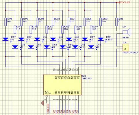
此模块由发光二极管和一个锁存器组成。
数据由2812模块的低八位输入,锁存器的控制信号由2812模块输出,但经由CPLD模块译码后再控制锁存器。
四、实验步骤
1. 把2812模块小板插到大板上;
2. 在CCS2000环境中打开本实验的工程编译Example_crossled.prj,生成输出文件,通过仿真器把执行代码下载到DSP芯片;
3. 运行程序,发光二极管按交通灯方式点亮熄灭。
4. 参考源代码,自行修改程序,实现不同的交通灯控制方式。
五、实验心得体会
通过次实验中,使我掌握了 2812的指令系统和74HC573的使用方法。同时,使我掌握了DSP的IO操作使用方法。
实验程序见附录:
附录:
#include "include/DSP281x_Device.h" // DSP281x Headerfile Include File
#include "include/DSP281x_Examples.h" // DSP281x Examples Include File
// Prototype statements for functions found within this file.
void delay_loop(void);
void Gpio_select(void);
// Global variable for this example
main()
{
// Step 1. Initialize System Control:
// PLL, WatchDog, enable Peripheral Clocks
// This example function is found in the DSP281x_SysCtrl.c file.
InitSysCtrl();
// Specific clock setting for this example:
EALLOW;
EDIS;
// Step 2. Initalize GPIO:
// This example function is found in the DSP281x_Gpio.c file and
// illustrates how to set the GPIO to it's default state.
// InitGpio(); // Skipped for this example
// For this example use the following configuration:
Gpio_select();
// Step 3. Clear all interrupts and initialize PIE vector table:
// Disable CPU interrupts
DINT;
// Initialize the PIE control registers to their default state.
// The default state is all PIE interrupts disabled and flags
// are cleared.
// This function is found in the DSP281x_PieCtrl.c file.
InitPieCtrl();
// Disable CPU interrupts and clear all CPU interrupt flags:
IER = 0x0000;
IFR = 0x0000;
// Initialize the PIE vector table with pointers to the shell Interrupt
// Service Routines (ISR).
// This will populate the entire table, even if the interrupt
// is not used in this example. This is useful for debug purposes.
// The shell ISR routines are found in DSP281x_DefaultIsr.c.
// This function is found in DSP281x_PieVect.c.
InitPieVectTable();
// Step 4. Initialize all the Device Peripherals:
// This function is found in DSP281x_InitPeripherals.c
// InitPeripherals(); // Not required for this example
InitXintf(); // For this example, init the Xintf
// Step 5. User specific code, enable interrupts:
while(1)
{
GpioDataRegs.GPADAT.all =0xdc80;
Reg00=0x00;
delay_loop();
GpioDataRegs.GPADAT.all =0xec40;
Reg00=0x00;
delay_loop();
GpioDataRegs.GPADAT.all =0xf0c0;
Reg00=0x00;
delay_loop();
GpioDataRegs.GPADAT.all =0xec40;
Reg00=0x00;
delay_loop();
}
}
void delay_loop()
{
short i,j;
for (i = 0; i < 32767; i++)
{for (j = 0; j < 50; j++);}
}
void Gpio_select(void)
{
Uint16 var1;
Uint16 var2;
Uint16 var3;
var1= 0x0000; // sets GPIO Muxs as I/Os
var2= 0xFFFF; // sets GPIO DIR as outputs
var3= 0x0000; // sets the Input qualifier values
EALLOW;
GpioMuxRegs.GPAMUX.all=var1;
GpioMuxRegs.GPBMUX.all=var1;
GpioMuxRegs.GPDMUX.all=var1;
GpioMuxRegs.GPFMUX.all=var1;
GpioMuxRegs.GPEMUX.all=var1;
GpioMuxRegs.GPGMUX.all=var1;
GpioMuxRegs.GPADIR.all=var2; // GPIO PORTs as output
GpioMuxRegs.GPBDIR.all=var2; // GPIO DIR select GPIOs as output
GpioMuxRegs.GPDDIR.all=var2;
GpioMuxRegs.GPEDIR.all=var2;
GpioMuxRegs.GPFDIR.all=var2;
GpioMuxRegs.GPGDIR.all=var2;
GpioMuxRegs.GPAQUAL.all=var3; // Set GPIO input qualifier values
GpioMuxRegs.GPBQUAL.all=var3;
GpioMuxRegs.GPDQUAL.all=var3;
GpioMuxRegs.GPEQUAL.all=var3;
EDIS;
}
//===========================================================================
// No more.
//===========================================================================
步进电机控制实验
一、实验目的
1. 掌握2812通用IO口的使用方法;
2. 掌握2812对步进电机的控制。
二、实验设备
1. 一台装有CCS软件的计算机;
2. DSP实验箱(插上电机模块);
3. DSP硬件仿真器;
4. 示波器。
三、实验原理
步进电机工作原理,给步进脉冲电机就转,不给脉冲电机就不转,步进脉冲的频率越高,步进控制电机就转的越快;改变各相的通电方式可以改变电机的运行方式;改变通电顺序可以控制步进电机的运行方式;改变通电顺序可以控制步进电机的正反转。
步进电机的控制问题可以总结为两点:
1. 产生工作方式需要的时序脉冲;
2. 控制步进电机的速度使它始终遵循加速-匀速-减速的规律工作。
对于I/O口有二类寄存器:
1. 控制寄存器和数据方向寄存器,使用方法如下:首先确定引脚的功能,即IO控制器寄存器,为1表示引脚功能是原模块的功能,否则为IO功能。
2. 如果引脚被配置为IO功能,就需要确定它的方向:输入还是输出,。为1表示是输出引脚,否则是输入引脚。对于IO功能的输入或输出是通过读写相应的数据方向寄存器来实现。输入引脚对应读操作;输出引脚对应写操作。
四、实验步骤
1. 连接好DSP开发系统;
2. 本实验工程文件(Example_stepmotor.pjt),编译,下载程序到DSP;
运行程序,用观察步进电机运行方向和速度的变化;
五、实验心得体会
通过本次实验对于2812通用的IO口进一步熟悉实验,使我基本掌握了2812通用的IO口的使用方法,加深了对IO口的认识。本次实验的主要目的是通过2812对步进机的的控制,开始对于程序的设计没有头绪,通过查阅步进机控制的原理,结合有关资料才正式设计出程序,基本掌握了2812对步进机的控制,也更加熟悉了对DSP程序的设计,受益匪浅。
程序:
#include "include/DSP281x_Device.h" // DSP281x Headerfile Include File
#include "include/DSP281x_Examples.h" // DSP281x Examples Include File
// Prototype statements for functions found within this file.
void delay_loop(void);
void Gpio_select(void);
// Global variable for this example
short codetab[17]=
{0x0001,0x0002,0x0004,0x0008,0x0008,0x0004,0x0002,0x0001,
0x0001,0x0002,0x0004,0x0008,0x0001,0x0002,0x0004,0x0008,0x0000};
main()
{ short i,j;
// Step 1. Initialize System Control:
// PLL, WatchDog, enable Peripheral Clocks
// This example function is found in the DSP281x_SysCtrl.c file.
InitSysCtrl();
// Specific clock setting for this example:
EALLOW;
EDIS;
// Step 2. Initalize GPIO:
// This example function is found in the DSP281x_Gpio.c file and
// illustrates how to set the GPIO to it's default state.
// InitGpio(); // Skipped for this example
// For this example use the following configuration:
Gpio_select();
// Step 3. Clear all interrupts and initialize PIE vector table:
// Disable CPU interrupts
DINT;
// Initialize the PIE control registers to their default state.
// The default state is all PIE interrupts disabled and flags
// are cleared.
// This function is found in the DSP281x_PieCtrl.c file.
InitPieCtrl();
// Disable CPU interrupts and clear all CPU interrupt flags:
IER = 0x0000;
IFR = 0x0000;
// Initialize the PIE vector table with pointers to the shell Interrupt
// Service Routines (ISR).
// This will populate the entire table, even if the interrupt
// is not used in this example. This is useful for debug purposes.
// The shell ISR routines are found in DSP281x_DefaultIsr.c.
// This function is found in DSP281x_PieVect.c.
InitPieVectTable();
// Step 4. Initialize all the Device Peripherals:
// This function is found in DSP281x_InitPeripherals.c
// InitPeripherals(); // Not required for this example
InitXintf(); // For this example, init the Xintf
// Step 5. User specific code, enable interrupts:
GpioDataRegs.GPADAT.all=0;
Reg06=0x00;
while(1)
{
for(j=0;j<400;j++)
{
for(i=0;i<4;i++)
{
GpioDataRegs.GPADAT.all =codetab[i];
Reg06=0x00;
delay_loop();
}
}
for(j=0;j<400;j++)
{
for(i=4;i<8;i++)
{
GpioDataRegs.GPADAT.all =codetab[i];
Reg06=0x00;
delay_loop();
}
}
}
}
void delay_loop()
{
short i,j;
for (i = 0; i < 1000; i++)
{for (j = 0; j < 10; j++);}
}
void Gpio_select(void)
{
Uint16 var1;
Uint16 var2;
Uint16 var3;
var1= 0x0000; // sets GPIO Muxs as I/Os
var2= 0xFFFF; // sets GPIO DIR as outputs
var3= 0x0000; // sets the Input qualifier values
EALLOW;
GpioMuxRegs.GPAMUX.all=var1;
GpioMuxRegs.GPBMUX.all=var1;
GpioMuxRegs.GPDMUX.all=var1;
GpioMuxRegs.GPFMUX.all=var1;
GpioMuxRegs.GPEMUX.all=var1;
GpioMuxRegs.GPGMUX.all=var1;
GpioMuxRegs.GPADIR.all=var2; // GPIO PORTs as output
GpioMuxRegs.GPBDIR.all=var2; // GPIO DIR select GPIOs as output
GpioMuxRegs.GPDDIR.all=var2;
GpioMuxRegs.GPEDIR.all=var2;
GpioMuxRegs.GPFDIR.all=var2;
GpioMuxRegs.GPGDIR.all=var2;
GpioMuxRegs.GPAQUAL.all=var3; // Set GPIO input qualifier values
GpioMuxRegs.GPBQUAL.all=var3;
GpioMuxRegs.GPDQUAL.all=var3;
GpioMuxRegs.GPEQUAL.all=var3;
EDIS;
}
//===========================================================================
// No more.
//===========================================================================
一、实验目的
1. 要求学生掌握2812 PWM的使用方法;
2. 掌握2812对直流电机的控制。
二、实验设备
1. 一台装有CCS软件的计算机;
2. DSP实验箱;
3. DSP硬件仿真器;
4. 示波器。
三、实验原理
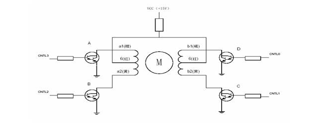
电机模块的原理图如下

四、实验步骤
3. 连接好DSP开发系统;
4. 本实验工程文件(Example_dcmotor.pjt),编译,下载程序到DSP;
5. 运行程序,用观察直流电机运行方向和速度的变化;
五、实验心得体会
通过本次实验,认识了PWM的使用方法,通过亲身体验,初步掌握了2812对PWM的控制使用方法,加深了对PWM的认识。本次实验的主要目的是通过2812对直流电机的控制,开始对于程序的设计没有头绪,通过查阅直流电机的原理,结合有关资料才正式设计出程序,基本掌握了2812对直流电机的控制,也更加熟悉了对DSP程序的设计,受益匪浅。
附:实验程序:
#include "include/DSP281x_Device.h" // DSP281x Headerfile Include File
#include "include/DSP281x_Examples.h" // DSP281x Examples Include File
// Prototype statements for functions found within this file.
void init_eva(void);
void init_evb(void);
void delay_loop();
// Global variable for this example
main()
{ unsigned short i;
// Step 1. Initialize System Control:
// PLL, WatchDog, enable Peripheral Clocks
// This example function is found in the DSP281x_SysCtrl.c file.
InitSysCtrl();
// Specific clock setting for this example:
EALLOW;
EDIS;
// Step 2. Initalize GPIO:
// This example function is found in the DSP281x_Gpio.c file and
// illustrates how to set the GPIO to it's default state.
// InitGpio(); // Skipped for this example
// Initialize only GPAMUX and GPBMUX for this test
EALLOW;
// Enable PWM pins
GpioMuxRegs.GPAMUX.all = 0x00FF; // EVA PWM 1-6 pins
GpioMuxRegs.GPBMUX.all = 0x00FF; // EVB PWM 7-12 pins
EDIS;
// Step 3. Clear all interrupts and initialize PIE vector table:
// Disable CPU interrupts
DINT;
// Initialize the PIE control registers to their default state.
// The default state is all PIE interrupts disabled and flags
// are cleared.
// This function is found in the DSP281x_PieCtrl.c file.
InitPieCtrl();
// Disable CPU interrupts and clear all CPU interrupt flags:
IER = 0x0000;
IFR = 0x0000;
// Initialize the PIE vector table with pointers to the shell Interrupt
// Service Routines (ISR).
// This will populate the entire table, even if the interrupt
// is not used in this example. This is useful for debug purposes.
// The shell ISR routines are found in DSP281x_DefaultIsr.c.
// This function is found in DSP281x_PieVect.c.
InitPieVectTable();
// Step 4. Initialize all the Device Peripherals:
// This function is found in DSP281x_InitPeripherals.c
// InitPeripherals(); // Not required for this example
InitXintf(); // For this example, init the Xintf
// Step 5. User specific code, enable interrupts:
init_eva();
//init_evb();
while(1)
{
for(i=0;i<65535;i+=1000)
{
Reg06=0;
EvbRegs.CMPR6 = i;
delay_loop();
}
}
}
void delay_loop()
{ short i,j;
for (i = 0; i < 1000; i++)
{for (j = 0; j < 10; j++);}
}
void init_eva()
{
// EVA Configure T1PWM, T2PWM, PWM1-PWM6
// Initalize the timers
// Initalize EVA Timer1
EvaRegs.T1PR = 0xFFFF; // Timer1 period
EvaRegs.T1CMPR = 0x3C00; // Timer1 compare
EvaRegs.T1CNT = 0x0000; // Timer1 counter
// TMODE = continuous up/down
// Timer enable
// Timer compare enable
EvaRegs.T1CON.all = 0x1042;
// Initalize EVA Timer2
EvaRegs.T2PR = 0x0FFF; // Timer2 period
EvaRegs.T2CMPR = 0x03C0; // Timer2 compare
EvaRegs.T2CNT = 0x0000; // Timer2 counter
// TMODE = continuous up/down
// Timer enable
// Timer compare enable
EvaRegs.T2CON.all = 0x1042;
// Setup T1PWM and T2PWM
// Drive T1/T2 PWM by compare logic
EvaRegs.GPTCONA.bit.TCMPOE = 1;
// Polarity of GP Timer 1 Compare = Active low
EvaRegs.GPTCONA.bit.T1PIN = 1;
// Polarity of GP Timer 2 Compare = Active high
EvaRegs.GPTCONA.bit.T2PIN = 2;
// Enable compare for PWM1-PWM6
//EvaRegs.CMPR1 = 0x0C00;
//EvaRegs.CMPR2 = 0x3C00;
EvaRegs.CMPR3 = 0xFC00;
// Compare action control. Action that takes place
// on a cmpare event
// output pin 1 CMPR1 - active high
// output pin 2 CMPR1 - active low
// output pin 3 CMPR2 - active high
// output pin 4 CMPR2 - active low
// output pin 5 CMPR3 - active high
// output pin 6 CMPR3 - active low
EvaRegs.ACTRA.all = 0x0666;
EvaRegs.DBTCONA.all = 0x0000; // Disable deadband
EvaRegs.COMCONA.all = 0xA600;
}
void init_evb()
{
// EVB Configure T3PWM, T4PWM and PWM7-PWM12
// Step 1 - Initialize the Timers
// Initialize EVB Timer3
// Timer3 controls T3PWM and PWM7-12
EvbRegs.T3PR = 0xFFFF; // Timer3 period
EvbRegs.T3CMPR = 0x3C00; // Timer3 compare
EvbRegs.T3CNT = 0x0000; // Timer3 counter
// TMODE = continuous up/down
// Timer enable
// Timer compare enable
EvbRegs.T3CON.all = 0x1042;
// Initialize EVB Timer4
// Timer4 controls T4PWM
EvbRegs.T4PR = 0x00FF; // Timer4 period
EvbRegs.T4CMPR = 0x0030; // Timer4 compare
EvbRegs.T4CNT = 0x0000; // Timer4 counter
// TMODE = continuous up/down
// Timer enable
// Timer compare enable
EvbRegs.T4CON.all = 0x1042;
// Setup T3PWM and T4PWM
// Drive T3/T4 PWM by compare logic
EvbRegs.GPTCONB.bit.TCMPOE = 1;
// Polarity of GP Timer 3 Compare = Active low
EvbRegs.GPTCONB.bit.T3PIN = 1;
// Polarity of GP Timer 4 Compare = Active high
EvbRegs.GPTCONB.bit.T4PIN = 2;
// Enable compare for PWM7-PWM12
EvbRegs.CMPR4 = 0x0C00;
EvbRegs.CMPR5 = 0x3C00;
EvbRegs.CMPR6 = 0xFC00;
// Compare action control. Action that takes place
// on a cmpare event
// output pin 1 CMPR4 - active high
// output pin 2 CMPR4 - active low
// output pin 3 CMPR5 - active high
// output pin 4 CMPR5 - active low
// output pin 5 CMPR6 - active high
// output pin 6 CMPR6 - active low
EvbRegs.ACTRB.all = 0x0666;
EvbRegs.DBTCONB.all = 0x0000; // Disable deadband
EvbRegs.COMCONB.all = 0xA600;
}
高速A/D转换实验
一、实验目的
1.了解高速 AD工作的基本原理。
2.了解如果通过软件正确的控制高速AD。
3.掌握对高速 AD正确操作的过程
二、实验设备
1. 一台装有CCS软件的计算机;
2. DSP实验箱;
3. DSP硬件仿真器;
三、实验原理
实验箱用的高速 AD 为 TLC5510,它是一个 CMOS 结构的、具有高达20MSPS 的8位模数转换器。TLC5510 采用单5V 供电,功耗仅为 130mW。TLC5510 内部包含有一个采样保持电路、具有高阻输出的并行接口以及内部参考电压等。
TLC5510 采用半 FlASh 结构,与 FlASh 结构相比,它不仅减少了功耗,而且提高了芯片的集成度。TLC5510 采用两步转换实现一次完整的转换,这样就大大减少了内部比较器的个数,其输出数据的延迟为2.5个时钟周期。TLC5510 采用 3 个内部参考电阻产生一个标准2V的参考电压,要实现内部参考电压仅需要通过外部的简单连线即可。TLC5510 的功能框图如图所示。
TLC5510内部有一个高位采样比较器和两个低位采样比较器。如图3-36所示,输入的电压 VI(1)在 CLK1 的上升沿被采样到高位比较器和低位比较器(A),对应的值为 S(1)。高位比较器在 CLK2 上升沿的时候完成高位数据UD(1)的转换,与此同时,根据高位数据产生了低位的参考电压 RV(1),低位比较器(A)在 CLK3 的上升沿完成完成低位数据 LD(1)的转换。在 CLK4的上升沿,高位数据 UD(1)和低位数据 LD(1)组成一个完整的数据 OUT(1)输出。整个数据的输出与输入的电压采样点相比有 2.5 个时钟周期的延迟。
输入电压VI(2)在CLK2的上升沿被采样,UD(2)在CLK3的上升沿完成,LD(2)在由低位比较器(B)在 CLK4 的上升沿完成,最终数据 OUT(2)在 CLK5的上升沿完成。
四、实验步骤
1. 连接好DSP开发系统,跳线连接高速AD输入和信号发生模块的输出;
2. 调节信号发生模块的工作频率和幅度;
3. 本实验工程文件(Example_hsad.pjt),编译,下载程序到DSP;
4. 运行程序,用观察A/D数据的变化;
五、实验心得体会
通过本次A/D转换实验,对于A/D信号的发生有了认识,使我掌握了高速 AD工作的基本原理和通过软件正确的控制高速AD。 同时掌握了对高速 AD正确操作的过程。
实验程序:
#include "include/DSP281x_Device.h"
#include "include/DSP281x_Examples.h"
// Prototype statements for functions found within this file.
void scia_loopback_init(void);
void scia_fifo_init(void);
void scia_xmit(int a);
void error(int);
interrupt void scia_rx_isr(void);
interrupt void scia_tx_isr(void);
// Global counts used in this example
Uint16 LoopCount;
Uint16 ErrorCount;
void main(void)
{ Uint16 SendChar;
Uint16 ReceivedChar;
// Step 1. Initialize System Control registers, PLL, WatchDog, Clocks to default state:
// This function is found in the DSP281x_SysCtrl.c file.
InitSysCtrl();
// Step 2. Select GPIO for the device or for the specific application:
// This function is found in the DSP281x_Gpio.c file.
// InitGpio(); skip this as this is example selects the I/O for SCI in this file itself
EALLOW;
GpioMuxRegs.GPFMUX.all=0x0030; // Select GPIOs to be Sci pins
// Port F MUX - x000 0000 0011 0000
EDIS;
// Step 3. Initialize PIE vector table:
// The PIE vector table is initialized with pointers to shell Interrupt
// Service Routines (ISR). The shell routines are found in DSP281x_DefaultIsr.c.
// Insert user specific ISR code in the appropriate shell ISR routine in
// the DSP28_DefaultIsr.c file.
// Disable and clear all CPU interrupts:
DINT;
IER = 0x0000;
IFR = 0x0000;
// Initialize Pie Control Registers To Default State:
// This function is found in the DSP281x_PieCtrl.c file.
// InitPieCtrl(); PIE is not used for this example
// Initialize the PIE Vector Table To a Known State:
// This function is found in DSP281x_PieVect.c.
// This function populates the PIE vector table with pointers
// to the shell ISR functions found in DSP281x_DefaultIsr.c.
InitPieVectTable();
// Enable CPU and PIE interrupts
// This example function is found in the DSP281x_PieCtrl.c file.
EnableInterrupts();
// Step 4. Initialize all the Device Peripherals to a known state:
// This function is found in DSP281x_InitPeripherals.c
// InitPeripherals(); skip this for SCI tests
// Step 5. User specific functions, Reassign vectors (optional), Enable Interrupts:
LoopCount = 0;
ErrorCount = 0;
scia_fifo_init(); // Initialize the SCI FIFO
scia_loopback_init(); // Initalize SCI for digital loop back
// Note: Autobaud lock is not required for this example
// Send a character starting with 0
SendChar = 0;
// Step 6. Send Characters forever starting with 0x00 and going through
// 0xFF. After sending each, check the recieve buffer for the correct value
for(;;)
{ scia_xmit(SendChar);
while(SciaRegs.SCIFFRX.bit.RXFIFST !=1) { } // wait for XRDY =1 for empty state
// Check received character
ReceivedChar = SciaRegs.SCIRXBUF.all;
if(ReceivedChar != SendChar) error(1);
// Move to the next character and repeat the test
SendChar++;
// Limit the character to 8-bits
SendChar &= 0x00FF;
LoopCount++;
if(LoopCount==256)
{
LoopCount=0;
SciaRegs.SCICCR.bit.LOOPBKENA =0; // Disable loop back
SciaRegs.SCICTL1.all =0x0023; // Relinquish SCI from Reset
while((ReceivedChar = SciaRegs.SCIRXBUF.all)!=0x0d);
scia_loopback_init(); // Initalize SCI for digital loop back
}
}
}
// Step 7. Insert all local Interrupt Service Routines (ISRs) and functions here:
void error(int ErrorFlag)
{ ErrorCount++;
// asm(" ESTOP0"); // Uncomment to stop the test here
// for (;;);
}
// Test 1,SCIA DLB, 8-bit word, baud rate 0x000F, default, 1 STOP bit, no parity
void scia_loopback_init()
{ // Note: Clocks were turned on to the SCIA peripheral
// in the InitSysCtrl() function
SciaRegs.SCICCR.all =0x0007; // 1 stop bit, No loopback
// No parity,8 char bits,
// async mode, idle-line protocol
SciaRegs.SCICTL1.all =0x0003; // enable TX, RX, internal SCICLK,
// Disable RX ERR, SLEEP, TXWAKE
SciaRegs.SCICTL2.all =0x0003;
SciaRegs.SCICTL2.bit.TXINTENA =1;
SciaRegs.SCICTL2.bit.RXBKINTENA =1;
SciaRegs.SCIHBAUD =0x0001;
SciaRegs.SCILBAUD =0x00e7;
SciaRegs.SCICCR.bit.LOOPBKENA =1; // Enable loop back
SciaRegs.SCICTL1.all =0x0023; // Relinquish SCI from Reset
}
// Transmit a character from the SCI'
void scia_xmit(int a)
{ SciaRegs.SCITXBUF=a;
}
// Initalize the SCI FIFO
void scia_fifo_init()
{ SciaRegs.SCIFFTX.all=0xE040;
SciaRegs.SCIFFRX.all=0x204f;
SciaRegs.SCIFFCT.all=0x0;
}
//===========================================================================
// No more.
//===========================================================================