DSP技术及应用课程设计报告
学院:通信与信息工程学院
专业: 电子信息工程专业
班级: 电信****班
姓名: 艾依河里的鱼
时间: 20##年1月1日
一、设计任务及要求
设计任务:本课程设计要求应用DES5402PP-U实验板实现FIR滤波器,能够在CCS集成开发环境中使用图形显示工具显示输入和输出波形。
设计要求:利用DES5402PP评估板的模拟信号输出通道产生一个1kHz的方波,然后将产生的方波信号通过模拟信号输入通道输入DES5402PP-U实验板,对方波进行低通滤波,得到一个1kHz的正弦信号。
二、设计原理
本设计中我们使用一个38阶的对称结构的FIR低通滤波器,其采样频率Fs为25KHz,通带截止频率1.2KHz,阻带截止频率为2.8KHz,阻带衰减为40DB。
我们可以应用MATLAB中的设计FIR滤波器的指令fir(),也可以应用MATLAB的工具FDATOOL来进行设计,然后将所设计的滤波器的系数导入DSP程序中。下面对FDATOOL进行简单的介绍:
FDATOOL(The Filter Design and Analysis Tool)是一个设计分析滤波器的工具,它具有很好的用户界面。借助它可以快速的设计数字IIR或FIR滤波器。你可以设置滤波器的性能指标,也可以直接配置滤波器的系数,还可以从MATLAB工作空间导入滤波器。在FDATOOL界面下,你可以方便的看到设计的滤波器的幅频特性、相频特性、零极点分布、单位脉冲响应、阶跃响应、滤波器系数、群时延等。
要使用FDATOOL,只要在MATLAB命令窗口中键入,按回车即可。FDATOOL有两种模式:设计模式和输入模式。在设计模式中,你可以从零开始设计,或者对已经设计的滤波器进行改进,或者分析滤波器。在输入模式中,你可以导入先前已经设计好的滤波器或者已经存在于MATLAB工作空间的滤波器系数,你还可以分析导入的滤波器。
本设计中我们主要使用FDATOOL的设计模式进行FIR滤波器的设计和对所设计的滤波器进行分析,然后可以用file菜单下的export将滤波器的系数导入MATLAB的Workspace和将系数写入DSP汇编程序中。在写系数到汇编程序中,要注意小数的表示方法。
三、程序代码
.title "fir5402.asm"
.ref _c_int00
.mmregs
;寄存器地址设置
gpiocr .set 3ch ;5402通用I/O控制寄存器
gpiosr .set 3dh ;5402通用I/O状态寄存器
dxr10 .set 23h ;串口0数据发送寄存器
drr10 .set 21h ;串口0数据接收寄存器
spsa0 .set 38h ;串口0子地址寄存器
spcr10 .set 39h ;多通道串口0寄存器1
spcr20 .set 39h ;多通道串口0寄存器2
xcr10 .set 39h ;串口0发送控制寄存器
pcr0 .set 39h ;串口0引脚控制寄存器
dxr11 .set 43h ;串口1数据发送寄存器
spsa1 .set 48h ;串口1子地址寄存器
spcr11 .set 49h ;多通道串口1寄存器1
spcr21 .set 49h ;多通道串口1寄存器2
xcr11 .set 49h ;串口1发送控制寄存器
pcr1 .set 49h ;串口1引脚控制寄存器
srgr1 .set 49h ;采样率发生寄存器1
srgr2 .set 49h ;采样率发生寄存器2
swcr .set 2bh ;软件等待状态寄存器
;定义变量
timer_count .set 060h ;定时器计数
mcbsp_init .set 061h ;mcbsp初始化
wave_ptr .set 062h
is_new_data .set 063h ;新数据到达标志
new_ad .set 064h
out_wave_ptr .set 065h
t_ar2 .set 066h
t_ar3 .set 067h
temp .set 068h
wave_buf .set 0900h
out_wave_buf .set 01000h
N .set 38 ; FIR taps
fir_coef_buf .set 100h ; FIR coef buffer
fir_data .set 200h ; FIR windows data buffer !
.text
;--------------------------------------------------------------------
; interrupt vector table !
;--------------------------------------------------------------------
rs b _c_int00
nop
nop
nmi b __ret
nop
nop
sint17 b __ret
nop
nop
sint18 b __ret
nop
nop
sint19 b __ret
nop
nop
sint20 b __ret
.word 0,0
sint21 b __ret
.word 0,0
sint22 .word 01000h
.word 0,0,0
sint23 .word 0ff80h
.word 0,0,0
sint24 .word 01000h
.word 0,0,0
sint25 .word 0ff80h
.word 0,0,0
sint26 .word 01000h
.word 0,0,0
sint27 .word 0ff80h
.word 0,0,0
sint28 .word 01000h
.word 0,0,0
sint29 .word 0ff80h
.word 0,0,0
sint30 .word 01000h
.word 0,0,0
int0 b __ret
nop
nop
int1 b __ret
nop
nop
int2 b __ret
nop
nop
tint b timer ;内部定时中断
nop
nop
brint0 b receive ;缓冲串口接收中断
nop
nop
bxint0 b transmit ;缓冲串口发送中断
nop
nop
trint b __ret
nop
nop
txint b __ret
nop
nop
int3 b __ret
nop
nop
hpint b __ret
nop
nop
q26 .word 0ff80h
.word 0,0,0
q27 .word 01000h
.word 0,0,0
q28 .word 0ff80h
.word 0,0,0
q29 .word 01000h
.word 0,0,0
q30 .word 0ff80h
.word 0,0,0
q31 .word 01000h
.word 0,0,0
;--------------------------------------------------------------------
; 复位中断服务程序
;--------------------------------------------------------------------
_c_int00:
stm #2020h,pmst ; vector table start: 0x2000,看IPTR中的值
ssbx intm ; close all int ! (ssbx intm)
ssbx sxm ; extend sign !
ssbx frct ; faction multiply
stm #10h,26h ; stop TIMER0 !
stm #10h,36h ; stop TIMER1 !
stm #0ffh,sp ; sp= 0x0ff
ld #0,dp ; dp=0
stm #0ffffh,ifr ; clear all int ! 中断标志寄存器
stm #20h,imr ; bit5->BXINT0, bit4->BRINT0, enable BXINT0
;中断屏蔽寄存器
stm #02492h,swwsr ; all 2 waits !
stm #0,swcr
;/*------------------------------------------------------------------
; 配置DSP的时钟
DES5402PP-U板的上电默认配置没有将DSP的时钟设置到100M,而只有20M。下面的程序将PLL改为×10,以便DSP以100M全速运行。PLL的时钟工作方式寄存器CLKMD,地址为0058H,见《DSP技术及应用》教材248页。
;------------------------------------------------------------------*/
stm #0,58h
wait_pll:
ldm 58h,a
and #1,a
bc wait_pll,aneq
stm #97ffh,58h ; switch pll*10 -> 100M clk
rpt #100
nop
;********************************************************************
;初始化RAM, Variable....
;********************************************************************
stm #wave_buf,ar6
stm #1,ar0
rpt #24
mvpd wave_data,*ar6+0 ; move wave data to wave_buf -> 0x0900h
stm #wave_buf,wave_ptr ; save wave buffer'ptr
stm #out_wave_buf,out_wave_ptr ; save out wave buffer'ptr, because use
; circular address, so when save out_wave
; date,must ++ !
stm #fir_coef_buf,ar6
rpt #N-1
mvpd fir_coef,*ar6+ ; move fir coef to fir_coef_buf(in data mem)
stm #fir_coef_buf,t_ar2 ;
stm #fir_data,t_ar3
stm #0aa55h,mcbsp_init ; when mcbsp_init==0xaa55, transmit for init ac01
stm #5,timer_count ; init variable timer_count !
stm #0,is_new_data ; if is_new_data ==1 , has new AD data by slave ac01 !
stm #1000h,ar0
stm #1800h,ar5
stm #400h,bk
ld *ar0,t
ld #0,b
;**************************************************************
; The following codes are used to initalize McBSP0 !
;***************************************************************
;-------------------------------------------------------------------
stm #0,spsa0 ; spsa0为串口0的子地址寄存器,choose SPCR10
stm #2000h,spcr10 ; receive sign_extend in DRR
stm #1,spsa0 ; choose SPCR20
stm #0c0h,spcr20 ; fs -> int !
stm #2,spsa0 ; choose RCR10
stm #40h,39h
stm #3,spsa0 ; choose RCR20
stm #0,39h
stm #4,spsa0 ; choose XCR10
stm #40h,xcr10
stm #5,spsa0 ; choose XCR20
stm #0,39h
stm #0eh,spsa0 ; choose PCR0
stm #0dh,pcr0 ; fs is low active, rise edge of clkx, falling edge
; of clkr
stm #7h,spsa0
stm #8000h,39h
rpt #0ffffh
nop
stm #00h,dxr10
ldm 22h,a
stm #1,38h
stm #0c1h,39h ; start McBSP0 send !
ld #603h,a
rsbx intm ; enable all int !
;--------------------------------------------------------------------
; The following codes initalizeAC01, ALL AC01 setup same !
;--------------------------------------------------------------------
idle 1
idle 1
idle 1
idle 1 ; 软件复位两个AC01
ld #600h,a
idle 1 ; wait for int .....
ld #3,a
idle 1 ; send #3
ld #00105h,a ; fs=10M/2/A/B= 25k
; flp=10M/2/40/A= 25k (all pass)
; fhp=fs/200= 125Hz (not use !)
; A=05,B=40(0x28)
idle 1 ; 送05h到AC01的数据寄存器1
ld #3,a
idle 1 ; send #3
ld #00228h,a
idle 1 ; 送28h到AC01的数据寄存器2
ld #3,a
idle 1 ; send #3
ld #00300h,a
idle 1 ; 送00h到AC01的数据寄存器3
ld #3,a
idle 1 ; send #3
ld #00405h,a
idle 1 ; 送05h 到AC01的数据寄存器4(AD & DA 0 dB)
ld #3,a
idle 1 ; send #3
ld #00505h,a
idle 1 ;送05h到AC01的数据寄存器5(highpass filter ;disable)
ld #3,a
idle 1 ; send #3
ld #00600h,a
idle 1 ; 送00h 到AC01的数据寄存器6
ld #3,a
idle 1 ; send #3
ld #00700h,a
idle 1 ; 送0到AC01的数据寄存器7
ld #3,a
idle 1 ; send #3
ld #800h,a
idle 1 ; 送0到AC01的数据寄存器8
ld #0h,a
stm #0,38h
stm #2001h,39h ;开始MCbsp0 接收!
stm #30h,imr ; bit5->BXINT0, bit4->BRINT0, 使能 BXINT0
;--------------------------------------------------------------------
;***************************************************************
; The following codes are used to initalize TIMER !
;***************************************************************
;--------------------------------------------------------------------
stm #10h,tcr ; stop TIMER !
stm #0ffffh,prd ;装载PRD, 周期寄存器
stm #0fh,tcr ; TIMER start, each about 100HZ ....
orm #8,imr ; enable TIMER INT !
;--------------------------------------------------------------------
;*************************************************** *********
; The following codes are main function
;**************************************************** ********
main:
bitf is_new_data,#1 ; test is_new_data == 1 ?
cc fir,tc ;==1, then call fir ! new AD data in new_ad(0x64)
b main ;检测到新数据到达标志(变量is_new_data)为1时,调
;用fir滤波程序。
;*************************************************** *********
; The following codes are served for McBSP0' transmit !
;**************************************************** ********
;--------------------------------------------------------------------
transmit:
pshm st1
pshm st0
pshm bk
pshm ar7
pshm ah
pshm al
cmpm mcbsp_init,#0aa55h
bc init,tc
stm #25,bk ; each AC01 has 25 dots to D/A !
mvdm #wave_ptr,ar7 ; restore wave buffer ptr !
nop
ld *ar7+%,a
nop
stlm a,dxr10 ; send wave data ! Master AC01 make source wave
; Slave AC01 make filter result wave !
bd wave_make_end
mvmd ar7,#wave_ptr ; save wave buffer ptr !
init:
stlm a,dxr10
bitf dxr10,#800h ; if setup last register of AC01, set mcbsp_init=0 !
bc wave_make_end,ntc ; not equal ,jump !
stm #0,mcbsp_init ; when mcbsp==0 or 1, transmit for make wave !
wave_make_end:
popm al
popm ah
popm ar7
popm bk
popm st0
popm st1
__ret:
rete
;--------------------------------------------------------------------
;********************************************************************
; The following codes are serived for McBSP0' receive ! use AR5,BK!
;********************************************************************
;--------------------------------------------------------------------
receive:
pshm st1
pshm st0
ld #0,dp
mvkd drr10,ar5 ; save AD data
pshd *ar5+% ; save AD data in AD_buffer(0x1800-0x1c00)
popd new_ad
stm #1,is_new_data ; has new AD data
popm st0
popm st1
rete
---------------------------------------------------------------------
;********************************************************************
; The following codes are serived for vc5402' TIMER !
;********************************************************************
;--------------------------------------------------------------------
timer:
pshm ah
pshm al
ldm timer_count,a
sub #1,a
bc not_show_led,aneq ; if a != 0 ,jump !
bitf st1,#2000h ; test XF
bc show_led,tc
ssbx xf ; set xf=1
b show_con
show_led
rsbx xf ; set xf=0
show_con
ld #5,a ;
not_show_led
stlm a,timer_count
popm al
popm ah
rete
;--------------------------------------------------------------------
;********************************************************************
; The following codes is used to FIR( new AD DATA in new_ad(0x64)
; FIR buffer coff-> 0x100(ar2), FIR window buffer -> 0x200(ar3))
;********************************************************************
fir:
pshm st1
pshm st0
pshm bk
pshm ar7
pshm ah
pshm al
pshm ar0
pshm ar2
pshm ar3
mvdm #t_ar2,ar2 ; restore ar2
mvdm #t_ar3,ar3 ; restore ar3
ld new_ad,-2,a ; new AD data -> a, remove two LSBs
;-------------------------------------------------------------------
stm #1,ar0
stm #N,bk ; set circular addressing size
stl a,*ar3+%
rptz a,#(N-1) ; 0 - a, then repeat 34 times
mac *ar2+0%,*ar3+0%,a ; done FIR filter, result in ah
mvmd ar3,#t_ar3 ; save ar3
mvmd ar2,#t_ar2 ; save ar2
stm #1,ar0
stm #100h,bk ; each AC01 has 25 dots to DA !
mvdm #out_wave_ptr,ar7 ; restore wave buffer ptr !
sth a,-2,temp ; save FIR result in temp
ld temp,2,a ; shift 2 bit for AC01 DA !
stl a,*ar7+0% ; save FIR result to wave buffer !
stl a,temp
mvmd ar7,#out_wave_ptr ; save wave buffer ptr !
stm #0,is_new_data ; new AD data has been processed !
ld #0,dp
cmpm out_wave_ptr, 1000h
bc con_fir,ntc
;-------------------------------------------------------------------
ccs_show: ;此处加断点,查看结果
nop ; if out_wave_ptr == 0xc00,
nop ; may show out_wave in CCS !!! show 128 dots !
; input buffer -> 0x1800
; output buffer -> 0x1000 (show from 0x1020)
con_fir:
popm ar3
popm ar2
popm ar0
popm al
popm ah
popm ar7
popm bk
popm st0
popm st1
ret
;********************************************************************
; The following data is used by make wave ! when using, must copy to
; wave buffer -> 0x6000
;********************************************************************
wave_data: ; freq about 1k Hz
.word 03ffch ; +2 volt
.word 03ffch
.word 03ffch
.word 03ffch
.word 03ffch
.word 03ffch
.word 03ffch
.word 03ffch
.word 03ffch
.word 03ffch
.word 03ffch
.word 03ffch
.word 03ffch
.word 0c000h ; -2 volt
.word 0c000h
.word 0c000h
.word 0c000h
.word 0c000h
.word 0c000h
.word 0c000h
.word 0c000h
.word 0c000h
.word 0c000h
.word 0c000h
.word 0c000h
;********************************************************************
; 滤波器的系数
Filter Type Lowpass
; Filter Length N
; Sampling Frequency 25.00000000
; Upper Band Edge 同学自行设计
; Lower Band Edge 同学自行设计
(在将滤波器系数写入DSP程序时注意小数的表示方法!)
;********************************************************************
fir_coef:
.word -50 ;c037
.word 101
.word 150
.word 203
.word 216
.word 153
.word -3
.word -239
.word -508
.word -729
.word -802
.word -634
.word -163
.word 615
.word 1638
.word 2777
.word 3861
.word 4711
.word 5178
.word 5178
.word 4711
.word 3861
.word 2777
.word 1638
.word 615
.word -163
.word -634
.word -802
.word -729
.word -508
.word -239
.word -3
.word 153
.word 216
.word 203
.word 150
.word 101
.word -50 ;c000
.end
四、调试步骤
1.短接JP9,使得DES5402PP的信号输出通道和输入通道相连。
2.启动CCS,新建一个工程fir5402.pjt。
3.在工程中添加文件fir5402.asm和 文件*.cmd,在标号ccs_show处添加断点,编译连接,然后将OUT文件装入,按Animate按钮运行程序。这时会看到断点处黄色箭头一直闪烁,状态栏有go字一直闪烁。
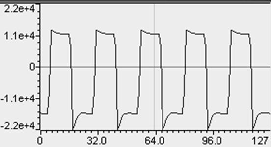
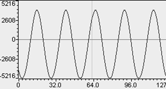
4.选择View->graph->Time/Frequency菜单打开一个图形显示窗口,参见下图。在“Start Address”项改为地址0x1800,将“Display Size”项设置128,将“DSP Data Type”改为“16-bitsigned integer”。这样,将在图形显示窗口中显示从0x1800(信号输入缓冲)开始的128个点的16位有符号整数。再打开一个图形窗口,显示从地址0x1020(滤波信号输出缓冲)开始的128个点的16位有符号整数。
五、实验结果
六、实验心得