石河子大学
毕业论文(设计)开题报告
课题名称: 基于单片机的电梯控制系统设计
学生姓名:
学 号: 2010509038
学 院: 机械电气工程学院
专业、年级:电气工程及其自动化2010(2)班
指导教师:
职 称: 副教授
毕业论文(设计)起止时间:1.10——6.15
文献综述
摘 要
电梯控制系统设计文献综述
1 电梯的定义及历史回眸
1.1 电梯的定义
一种以电动机为动力的垂直升降机,装有箱状吊舱,用于多层建筑乘人或载运货物。也有台阶式,踏步板装在履带上连续运行,俗称自动电梯。它是服务于规定楼层的固定式升降设备。具有一个轿厢,运行在至少两列垂直的或倾斜角小于15°的刚性导轨之间。轿厢尺寸与结构形式便于乘客出入或装卸货物。
习惯上不论其驱动方式如何,将电梯作为建筑物内垂直交通运输工具的总称。
1.2 电梯的发展历史回眸
电梯技术发展大致分为两个阶段[1]:
(1)电梯的雏形阶段
1785年,英国出现了用蒸汽机驱动的升降机;1900年,以交流电动机传动的电梯开始问世。1902年,瑞士的迅达公司研制成功了世界上第一台按钮式自动电梯,采用全自动的控制方式,提高了电梯的输送能力和安全性。
(2)现代电梯的发展阶段
1903年,美国奥的斯公司生产了不带减速器的无齿轮高速电梯,电梯传动机构采用曳引驱动代替以往的卷筒式,为当今高层的大行程、高速度电梯奠定了基础;1976年,电梯上开始运用微处理机,之后随着大功率晶体管模块的问世,以及微机及数字调节器技术的不断成熟,人们利用调节脉冲宽度来调节电子逆变器,实现了对电梯中电动机的调压调频(VVVF),达到了线性调速的目的;1990年,电梯控制系统由并行信号传输向以串行为主的信号传输过渡,提高了整体系统的可靠性,为实现电梯的群控,智能化和远程监控提供了条件。
1.3 我国电梯事业的发展现状[2]
大规模的经济建设尤其是蓬勃发展的房地产业给电梯行业开拓了广阔的市场,20##年我国电梯产量达4.5万台,创造了行业发展史上的一个新的高峰,被业内人士称为“第三次浪潮”。目前,中国经济建设需求的各类电梯、几乎全部可以在中国生产。据统计,全世界平均1000人有1台电梯。我国如果要达到这个水准,还需要新装80万台。到那时候,每年仅报废更新就需要6万台。目前房屋建设势头仍然很好,电梯市场供需两旺,前景一片光明。
2 电梯技术发展趋势展望[3] [4] [5] [6]
电梯的普及给人们的生活带来了极大的优越性,而电梯技术也只有不断的发展才能更好地满足高层建筑及其群体的需要。展望未来,电梯的发展趋势应包括以下几点:
2.1 无机房电梯
无机房电梯不单单是电梯有无机房的简单局部改进,而是涉及到一系列技术问题,如曳引系统、控制柜、限速器等的安装位置以及轿厢、极限开关、缓冲器等部件,都要进行重新设计,变更部件的尺寸与安装位置也要重新考虑。它是电梯发展过程中的一次意义深远的变革,它所采用的一些关键技术将会被进一步推广用到其它电梯产品上,进而促进整个电梯行业技术的进步。
2.2 绿色电梯
绿色电梯的研究主要在电梯制造、配置及安装、使用过程中节能和减少环境污染等方面。节能主要体现在以下几个方面:原材料的充分利用;电梯数量与参数的优化配置;高效的驱动系统;减少机械系统的惯性和摩擦阻力;选用节能照明;客货流量规划等方面。减小对环境的污染主要体现在两方面:油污染降至最低;电梯的电磁兼容性问题。由于电梯是在大厦中频繁启动的大容量电器,由此产生的电磁辐射将对大楼的办公设备构成严重干扰。
2.3远程监控系统
远程监控系统的应用,使得电梯状态监控的智能可以在监控中心就可以监测到电梯的运行状态,监控中心随时可以监控电梯发生的故障,并且可以诊断出故障的类型和发生的位置,使电梯维护更加安全、方便。
2.4 全微机化电梯
全微机化电梯的开发和使用,是电梯发展趋势的一个重要方向。全微机化电梯是指电梯的传动系统及操纵控制系统方面实现微机控制的电梯。随着现代微机技术的不断进步和完善,全微机化电梯( 包括单微机控制电梯、多微机控制电梯及人工智能控制电梯) 必将全面满足人们对电梯高质量,高水平,高标准的要求。
2.6 太空电梯
1895年前苏联科学家设想坐电梯进入太空,后来一些科学家相继提出了各种解决方案。20##年,美国国家宇航局(NASA)描述了建造太空电梯的概念,这需要极细的碳纤维制成的缆绳并能延伸到地球赤道上方3.5万km。为使这条缆绳突破地心引力的影响太空中的另一端必须与一个质量巨大的天体相连。这一天体向外太空旋转的力量与地心引力抗衡,将使缆绳紧绷,允许电磁轿厢在缆绳中心的隧道穿行。普通人登上太空这个梦想未来将实现。
除以上几方面外,诸如IC卡的智能管理系统,应用模糊理论和神经网络技术的群管理系统,以及数码技术、声控技术、载波技术等也将在电梯技术领域中得到推广和发展。
4 电梯的控制技术[7] [8]
4.1电梯系统的控制
电梯的控制从性质上可以分为两个方面,一是其传动系统的控制,二是电梯逻辑控制。
(1) 传动系统的控制
它是以速度给定曲线为依据,利用模拟或数字控制装置,针对曳引电机的不同调速方式构成闭环或开环的速度控制系统,从而实现电梯运动状态的控制。
(2) 电梯的逻辑控制
电梯作为一种多层站、长距离的垂直交通工具,只对传动系统进行控制还不能满足实际运行的需要,它必须能实时的接受来自厅站、轿厢、井道、机房等不同位置、不同性质的外部信号,将它们按一定的逻辑关系进行综合处理,并将其处理结果反应到传动控制系统中控制电梯运行。例如,电梯同时接受到不同层站的召唤信号,其中有上行也有下行,那么应本着尽量减少电梯起动次数,缩短乘客侯梯时间的原则,使电梯先响应部分召唤,而把另一部分暂时记忆下来,待电梯响应完前一批召唤后,再响应所一记忆的另一部分召唤信号。这是电梯控制的另一方面,称为电梯逻辑控制,也称电梯逻辑操纵系统。
(3) 电梯逻辑控制的基本功能
轿内指令功能:由司机或乘客在轿箱内控制电梯的运行方向和到达层站。
厅外呼梯功能:由乘客或使用人员在厅外呼唤电梯前往该层执行运送任务。
减速平层功能:电梯达到目的层站前的某一位置时,能自动的使电梯开始减速,当到达目的层站平面时,能自动使电梯停止。
选层、定向功能:当电梯接受到若干个轿内、厅外指令时,能根据电梯目前的状态选择最合理的运行方式及停靠层站。
指示功能:能在各层厅站及轿厢中指示电梯当前所处位置,能在某按钮信号被响应时消去其记忆。
保护功能:当电梯出现异常,如出现超速、断绳、越限、运行中开门、过载等现象时,控制电梯停车或禁用。
检修功能:有检修开关、检修主令元件,便于检修人员在机房、轿顶或轿内独立控制电梯以检修方式运行。
4.2 电梯控制系统[10]
电梯控制系统主要采用以下三种方式:一是继电器控制系统、二是PLC控制系统、三是微机控制系统。继电器控制系统由于故障率高,控制方式不灵活及功率消耗大等缺点,目前已逐渐被人们所淘汰。微机控制系统虽然在智能控制方面有较强大的功能,但也存在一定的不足之处,即抗干扰性差,系统设计较复杂,一般维修人员难以掌握其维修技术,这些都限制了微机控制系统应用的广泛性。而PLC控制系统由于运行可靠、使用维修方便、抗干扰性强等优越性,成为目前在电梯控制系统中使用最多的控制方式。
4.2.1 电梯继电器控制系统的特点及存在问题
(1)系统的触点繁多、接线线路复杂,且触点容易烧坏磨损,造成接触不良,因而故障率较高。
(2)普通控制电器及硬件接线方法难以实现较复杂的控制功能,使系统的控制功能不易增加,技术水平难以提高。
(3)电磁机构及触点动作速度比较慢,机械和电磁惯性大,系统控制精度难以提高。
(4)系统结构庞大,能耗较高,机械动作噪音大。
(5)由于线路复杂,易出现故障,因而保养维修工作量大,费用高,而且检查故障困难,费时费工。
(6)电梯继电器控制系统故障率高,大大降低了电梯的可靠性和安全性,经常造成停梯,给乘用人员带来不便和惊忧。且电梯一旦发生冲顶或蹲底,不但会造成电梯机械部件损坏,还可能出现人身事故。
4.2.2 单片机在电梯控制中的应用特点
单片机以其卓越的性能,得到了广泛的应用,已深入到各个领域。单片机应用在检测、控制领域中,具有如下特点。
一、成本低。本电梯控制由于采用单片机代替了PLC作为主控芯片, 同时用PWM 驱动直流电机代替了变频调速驱动,从而导致整套系统成本很低。
二、高精度的重量检测及显示。基于PLC的电梯模型虽然有重量检测,但检测精度较低。本电梯模型采用高精度的重量传感器和测量电路, 配合设计优良的数字处理软件,从而能进行高精度的重量检测和显示.
三、 可靠性好,适应温度范围宽。单片机芯片本身是按工业测控环境要求设计的,能适应各种恶劣的环境,这是其它机种无法比拟的。
四、 易扩展,很容易构成各种规模的应用系统,控制功能强。单片机的逻辑控制功能很强,指令系统有各种控制功能用指令。
五、 可以很方便的实现多机和分布式控制。
六、 单片机可以构成形式多样的控制系统、数据采集系统。
参考文献
1 魏志精.可编程控制器应用基础【M】.电子工业出版社,2003
2 武锋.可编程控制器PLC的基本原理及应用[J].电子世界,2002,(11)
3 孟红军.三菱变频调速器FR-A500使用手册,2004
4 唐勇奇,赵葵银.电梯变频调速PLC控制的设计与实现[J].电机电器技术,2000
5张凤池.现代工厂电气控制[M].北京:机械工业出版社,2000
6 廖常初、PLC梯形图程序的设计方法与技巧、电工技术、1998-1999
[7 王永华.现代电气控制及可编程控制技术[M].北京航空航天出版社,2002
8 李世基.微机与可编程控制器[M].北京机械工业出版社,1994
9 郭肖永.浅谈PLC安全性[J].化工自动化及仪表,1998
10 张万忠.电器与PLC控制技术[M].北京化学工业出版社,2003
11 李方园.PLC工业应用实践[M].中国电力出版社,2001:12-58.
12 西门子(中国)有限公司.SIMATIC S-200可编程序控制器系统西门子手册.
AT89S52 MCU Applications
Function Characteristic Description
The AT89S52 is a low-power, high-performance CMOS 8-bit microcontroller with 8K bytes of in-system programmable Flash memory. The device is manufactured using Atmel’s high-density nonvolatile memory technology and is compatible with the indus-try-standard 80C51 instruction set and pinout. The on-chip Flash allows the program memory to be reprogrammed in-system or by a conventional nonvolatile memory pro-grammer. By combining a versatile 8-bit CPU with in-system programmable Flash on a monolithic chip, the Atmel AT89S52 is a powerful microcontroller which provides a highly-flexible and cost-effective solution to many embedded control applications.The AT89S52 provides the following standard features: 8K bytes of Flash, 256 bytes of RAM, 32 I/O lines, Watchdog timer, two data pointers, three 16-bit timer/counters, a six-vector two-level interrupt architecture, a full duplex serial port, on-chip oscillator, and clock circuitry. In addition, the AT89S52 is designed with static logic for operation down to zero frequency and supports two software selectable power saving modes. The Idle Mode stops the CPU while allowing the RAM, timer/counters, serial port, and interrupt system to continue functioning. The Power-down mode saves the RAM con-tents but freezes the oscillator, disabling all other chip functions until the next interrupt or hardware reset.
Pin Description
VCC :Supply voltage.
GND :Ground.
Port 0:Port 0 is an 8-bit open drain bidirectional I/O port. As an output port, each pin can sink eight TTL inputs. When 1s are written to port 0 pins, the pins can be used as high-impedance inputs. Port 0 can also be configured to be the multiplexed low-order address/data bus during accesses to external program and data memory. In this mode, P0 has internal pull-ups. Port 0 also receives the code bytes during Flash programming and outputs the code bytes dur-ing program verification. External pull-ups are required during program verification.
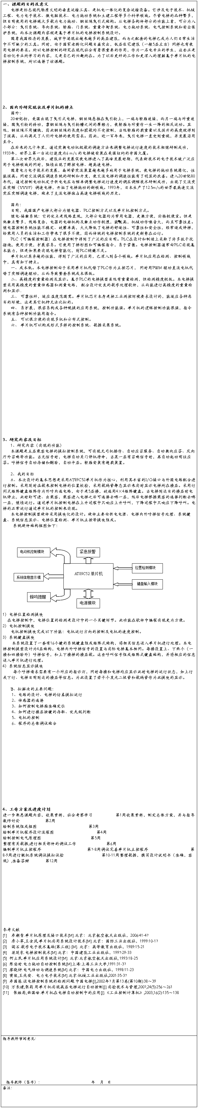
Port 1:Port 1 is an 8-bit bidirectional I/O port with internal pull-ups. The Port 1 output buffers can sink/source four TTL inputs. When 1s are written to Port 1 pins, they are pulled high by the inter-nal pull-ups and can be used as inputs. As inputs, Port 1 pins that are externally being pulled low will source current (IIL) because of the internal pull-ups. In addition, P1.0 and P1.1 can be configured to be the timer/counter 2 external count input (P1.0/T2) and the timer/counter 2 trigger input (P1.1/T2EX), respectively, as shown in the follow-ing table 1. Port 1 also receives the low-order address bytes during Flash programming and verification.
Table 1 The second function of the P1 port
Port 2:Port 2 is an 8-bit bidirectional I/O port with internal pull-ups. The Port 2 output buffers can sink/source four TTL inputs. When 1s are written to Port 2 pins, they are pulled high by the inter-nal pull-ups and can be used as inputs. As inputs, Port 2 pins that are externally being pulled low will source current (IIL) because of the internal pull-ups. Port 2 emits the high-order address byte during fetches from external program memory and dur-ing accesses to external data memory that use 16-bit addresses (MOVX @ DPTR). In this application, Port 2 uses strong internal pull-ups when emitting 1s. During accesses to external data memory that use 8-bit addresses (MOVX @ RI), Port 2 emits the contents of the P2 Special Function Register. Port 2 also receives the high-order address bits and some control signals during Flash program-ming and verification.
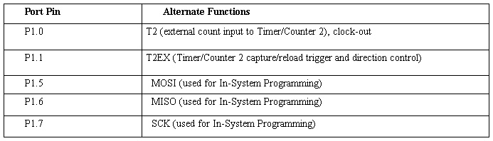
Port 3:Port 3 is an 8-bit bidirectional I/O port with internal pull-ups. The Port 3 output buffers can sink/source four TTL inputs. When 1s are written to Port 3 pins, they are pulled high by the inter-nal pull-ups and can be used as inputs. As inputs, Port 3 pins that are externally being pulled low will source current (IIL) because of the pull-ups. Port 3 receives some control signals for Flash programming and verification. Port 3 also serves the functions of various special features of the AT89S52, as shown in the fol-lowing table 2.
Table 2 The second function of the P3 port
RST:Reset input. A high on this pin for two machine cycles while the oscillator is running resets the device. This pin drives high for 98 oscillator periods after the Watchdog times out. The DISRTO bit in SFR AUXR (address 8EH) can be used to disable this feature. In the default state of bit DISRTO, the RESET HIGH out feature is enabled.
ALE/ :Address Latch Enable (ALE) is an output pulse for latching the low byte of the address during accesses to external memory. This pin is also the program pulse input (
 ) during Flash programming. In normal operation, ALE is emitted at a constant rate of 1/6 the oscillator frequency and may be used for external timing or clocking purposes. Note, however, that one ALE pulse is skipped dur-ing each access to external data memory. If desired, ALE operation can be disabled by setting bit 0 of SFR location 8EH. With the bit set, ALE is active only during a MOVX or MOVC instruction. Otherwise, the pin is weakly pulled high. Setting the ALE-disable bit has no effect if the microcontroller is in external execution mode.
 :Program Store Enable (
 ) is the read strobe to external program memory. When the AT89S52 is executing code from external program memory, is activated twice each machine cycle, except that two activations are skipped during each access to exter-nal data memory.
 /VPP:External Access Enable.
  must be strapped to GND in order to enable the device to fetch code from external program memory locations starting at 0000H up to FFFFH. Note, however, that if lock bit 1 is programmed, will be internally latched on reset. should be strapped to VCC for internal program executions. This pin also receives the 12-volt programming enable voltage (VPP) during Flash programming.
XTAL1:Input to the inverting oscillator amplifier and input to the internal clock operating circuit.
XTAL2:Output from the inverting oscillator amplifier.
Program Memory
If the pin is connected to GND, all program fetches are directed to external memory. On the AT89S52, if is connected to VCC, program fetches to addresses 0000H through 1FFFH are directed to internal memory and fetches to addresses 2000H through FFFFH are to external memory.
Data Memory
The AT89S52 implements 256 bytes of on-chip RAM. The upper 128 bytes occupy a parallel address space to the Special Function Registers. This means that the upper 128 bytes have the same addresses as the SFR space but are physically separate from SFR space. When an instruction accesses an internal location above address 7FH, the address mode used in the instruction specifies whether the CPU accesses the upper 128 bytes of RAM or the SFR space. Instructions which use direct addressing access the SFR space. For example, the following direct addressing instruction accesses the SFR at location 0A0H (which is P2). MOV 0A0H, #data. Instructions that use indirect addressing access the upper 128 bytes of RAM. For example, the following indirect addressing instruction, where R0 contains 0A0H, accesses the data byte at address 0A0H, rather than P2 (whose address is 0A0H).MOV @R0, #data. Note that stack operations are examples of indirect addressing, so the upper 128 bytes of data RAM are available as stack space.
Watchdog Timer
The WDT is intended as a recovery method in situations where the CPU may be subjected to software upsets. The WDT consists of a 14-bit counter and the Watchdog Timer Reset (WDTRST) SFR. The WDT is defaulted to disable from exiting reset. To enable the WDT, a user must write 01EH and 0E1H in sequence to the WDTRST register (SFR location 0A6H). When the WDT is enabled, it will increment every machine cycle while the oscillator is running. The WDT timeout period is dependent on the external clock frequency. There is no way to disable the WDT except through reset (either hardware reset or WDT overflow reset). When WDT over-flows, it will drive an output RESET HIGH pulse at the RST pin.
In Power-down mode the oscillator stops, which means the WDT also stops. While in Power-down mode, the user does not need to service the WDT. There are two methods of exiting Power-down mode: by a hardware reset or via a level-activated external interrupt which is enabled prior to entering Power-down mode. When Power-down is exited with hardware reset, servicing the WDT should occur as it normally does whenever the AT89S52 is reset. Exiting Power-down with an interrupt is significantly different. The interrupt is held low long enough for the oscillator to stabilize. When the interrupt is brought high, the interrupt is serviced. To prevent the WDT from resetting the device while the interrupt pin is held low, the WDT is not started until the interrupt is pulled high. It is suggested that the WDT be reset during the interrupt service for the interrupt used to exit Power-down mode. To ensure that the WDT does not overflow within a few states of exiting Power-down, it is best to reset the WDT just before entering Power-down mode. Before going into the IDLE mode, the WDIDLE bit in SFR AUXR is used to determine whether the WDT continues to count if enabled. The WDT keeps counting during IDLE (WDIDLE bit = 0) as the default state. To prevent the WDT from resetting the AT89S52 while in IDLE mode, the user should always set up a timer that will periodically exit IDLE, service the WDT, and reenter IDLE mode. With WDIDLE bit enabled, the WDT will stop to count in IDLE mode and resumes the count upon exit from IDLE.
Timer 0 and 1
Timer 0 and Timer 1 in the AT89S52 operate the same way as Timer 0 and Timer 1 in the AT89C51 and AT89C52. For further information on the timers’ operation, please click on the document link below:
http://www.atmel.com/dyn/resources/prod_documents/DOC4316.PDF
Timer 2
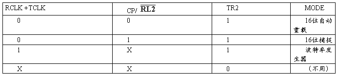
Timer 2 is a 16-bit Timer/Counter that can operate as either a timer or an event counter. The type of operation is selected by bit C/ in the SFR T2CON. Timer 2 has three operating modes: capture, auto-reload (up or down counting), and baud rate generator. The modes are selected by bits in T2CON, as shown in Table 6-1. Timer 2 consists of two 8-bit registers, TH2 and TL2. In the Timer function, the TL2 register is incremented every machine cycle. Since a machine cycle consists of 12 oscillator periods, the count rate is 1/12 of the oscil-lator frequency.
Table3 Timer 2 Operating Modes

In the Counter function, the register is incremented in response to a 1-to-0 transition at its corre-sponding external input pin, T2. In this function, the external input is sampled during S5P2 of every machine cycle. When the samples show a high in one cycle and a low in the next cycle, the count is incremented. The new count value appears in the register during S3P1 of the cycle following the one in which the transition was detected. Since two machine cycles (24 oscillator periods) are required to recognize a 1-to-0 transition, the maximum count rate is 1/24 of the oscillator frequency. To ensure that a given level is sampled at least once before it changes, the level should be held for at least one full machine cycle.
Interrupts
The AT89S52 has a total of six interrupt vectors: two external interrupts ( and
and  ), three timer interrupts (Timers 0, 1, and 2), and the serial port interrupt. Each of these interrupt sources can be individually enabled or disabled by setting or clearing a bit in Special Function Register IE. IE also contains a global disable bit, EA, which disables all interrupts at once. Note that bit position IE.6 is unimplemented. User software should not write a 1 to this bit position, since it may be used in future AT89 products. Timer 2 interrupt is generated by the logical OR of bits TF2 and EXF2 in register T2CON. Nei-ther of these flags is cleared by hardware when the service routine is vectored to. In fact, the service routine may have to determine whether it was TF2 or EXF2 that generated the interrupt, and that bit will have to be cleared in software. The Timer 0 and Timer 1 flags, TF0 and TF1, are set at S5P2 of the cycle in which the timers overflow. The values are then polled by the circuitry in the next cycle. However, the Timer 2 flag, TF2, is set at S2P2 and is polled in the same cycle in which the timer overflows.
Oscillator Characteristics
XTAL1 and XTAL2 are the input and output, respectively, of an inverting amplifier that can be configured for use as an on-chip oscillator. Either a quartz crystal or ceramic resonator may be used. To drive the device from an external clock source, XTAL2 should be left unconnected while XTAL1 is driven,. There are no requirements on the duty cycle of the external clock signal, since the input to the internal clock-ing circuitry is through a divide-by-two flip-flop, but minimum and maximum voltage high and low time specifications must be observed.
Power-down Mode
In the Power-down mode, the oscillator is stopped, and the instruction that invokes Power-down is the last instruction executed. The on-chip RAM and Special Function Registers retain their values until the Power-down mode is terminated. Exit from Power-down mode can be initiated either by a hardware reset or by an enabled external interrupt. Reset redefines the SFRs but does not change the on-chip RAM. The reset should not be activated before VCC is restored to its normal operating level and must be held active long enough to allow the oscillator to restart and stabilize.
Idle Mod
In idle mode, the CPU puts itself to sleep while all the on-chip peripherals remain active. The mode is invoked by software. The content of the on-chip RAM and all the special functions regis-ters remain unchanged during this mode. The idle mode can be terminated by any enabled interrupt or by a hardware reset. Note that when idle mode is terminated by a hardware reset, the device normally resumes pro-gram execution from where it left off, up to two machine cycles before the internal reset algorithm takes control. On-chip hardware inhibits access to internal RAM in this event, but access to the port pins is not inhibited. To eliminate the possibility of an unexpected write to a port pin when idle mode is terminated by a reset, the instruction following the one that invokes idle mode should not write to a port pin or to external memory.
AT89S52单片机应用
功能特征描述
AT89S52是一种低功耗、高性能CMOS8位微控制器,具有8K 在系统可编程Flash 存储器。使用Atmel 公司高密度非易失性存储器技术制造,与工业80C51 产品指令和引脚完全兼容。片上Flash允许程序存储器在系统可编程,亦适于常规编程器。在单芯片上,拥有灵巧的8 位CPU 和在系统可编程Flash,使得AT89S52为众多嵌入式控制应用系统提供高灵活、超有效的解决方案。 AT89S52具有以下标准功能: 8k字节Flash,256字节RAM,32 位I/O 口线,看门狗定时器,2个数据指针,三个16 位定时器/计数器,一个6向量2级中断结构,全双工串行口,片内晶振及时钟电路。另外,AT89S52 可降至0Hz 静态逻辑操作,支持2种软件可选择节电模式。空闲模式下,CPU停止工作,允许RAM、定时器/计数器、串口、中断继续工作。掉电保护方式下,RAM内容被保存,振荡器被冻结,单片机一切工作停止,直到下一个中断或硬件复位为止。
引脚描述
VCC :电源。
GND: 接地。
P0口: P0口是一个8位漏极开路的双向I/O口。作为输出口,每位能驱动8个TTL逻辑电平。对P0端口写“1”时,引脚用作高阻抗输入。当访问外部程序和数据存储器时,P0口也被作为低8位地址/数据复用。在这种模式下,P0具有内部上拉电阻。在flash编程时,P0口也用来接收指令字节;在程序校验时,输出指令字节。程序校验时,需要外部上拉电阻。
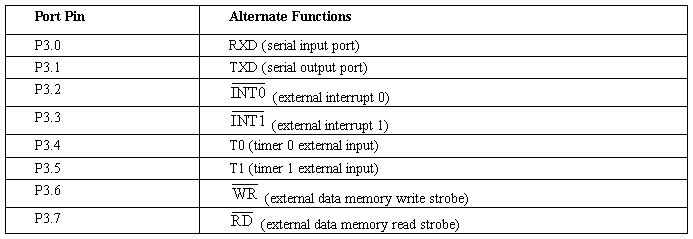
P1口:P1 口是一个具有内部上拉电阻的8 位双向I/O 口,p1 输出缓冲器能驱动4 个TTL 逻辑电平。对P1 端口写“1”时,内部上拉电阻把端口拉高,此时可以作为输入口使用。作为输入使用时,被外部拉低的引脚由于内部电阻的原因,将输出电流(IIL)。此外,P1.0和P1.2分别作定时器/计数器2的外部计数输入(P1.0/T2)和时器/计数器2的触发输入(P1.1/T2EX),具体如下表1所示。在flash编程和校验时,P1口接收低8位地址字节。
P2口:P2 口是一个具有内部上拉电阻的8 位双向I/O 口,P2 输出缓冲器能驱动4 个TTL 逻辑电平。对P2 端口写“1”时,内部上拉电阻把端口拉高,此时可以作为输入口使用。作为输入使用时,被外部拉低的引脚由于内部电阻的原因,将输出电(IIL)。在访问外部程序存储器或用16位地址读取外部数据存储器(例如执行MOVX @DPTR)时,P2 口送出高八位地址。在这种应用中,P2 口使用很强的内部上拉发送1。在使用8位地址(如MOVX @RI)访问外部数据存储器时,P2口输出P2锁存器的内容。在flash编程和校验时,P2口也接收高8位地址字节和一些控制信号。
表1 P1口第二功能
表2 P3口第二功能
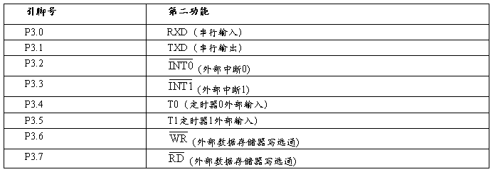
P3口:P3 口是一个有内部上拉电阻的8 位双向I/O 口,p2 输出缓冲器能驱动4 个TTL 逻辑电平。对P3 端口写“1”时,内部上拉电阻把端口拉高,此时可以作为输入口使用。作为输入使用时,被外部拉低的引脚由于内部电阻的原因,将输出电流(IIL)。P3口亦作为AT89S52特殊功能(第二功能)使用,如2表所示。在flash编程和校验时,P3口也接收一些控制信号。
RST:复位输入。晶振工作时,RST脚持续2 个机器周期高电平将使单片机复位。看门狗计时完成后,RST 脚输出96 个晶振周期的高电平。特殊寄存器AUXR(地址8EH)上的DISRTO位可以使此功能无效。DISRTO默认状态下,复位高电平有效。
ALE/ :地址锁存控制信号(ALE)是访问外部程序存储器时,锁存低8 位地址的输出脉冲。在flash编程时,此引脚(
 )也用作编程输入脉冲。在一般情况下,ALE 以晶振六分之一的固定频率输出脉冲,可用来作为外部定时器或时钟使用。然而,特别强调,在每次访问外部数据存储器时,ALE脉冲将会跳过。如果需要,通过将地址为8EH的SFR的第0位置 “1”,ALE操作将无效。这一位置 “1”,ALE 仅在执行MOVX 或MOVC指令时有效。否则,ALE 将被微弱拉高。这个ALE 使能标志位(地址为8EH的SFR的第0位)的设置对微控制器处于外部执行模式下无效。
 :外部程序存储器选通信号(
 )是外部程序存储器选通信号。当AT89S52从外部程序存储器执行外部代码时,在每个机器周期被激活两次,而在访问外部数据存储器时,将不被激活。
 /VPP:访问外部程序存储器控制信号。为使能从0000H 到FFFFH的外部程序存储器读取指令,
 必须接GND。为了执行内部程序指令,应该接VCC。在flash编程期间,也接收12伏VPP电压。
XTAL1:振荡器反相放大器和内部时钟发生电路的输入端。
XTAL2:振荡器反相放大器的输出端。
程序存储器
如果引脚接地,程序读取只从外部存储器开始。对于89S52,如果 接VCC,程序读写先从内部存储器(地址为0000H~1FFFH)开始,接着从外部寻址,寻址地址为:2000H~FFFFH。
数据存储器
AT89S52 有256 字节片内数据存储器。高128 字节与特殊功能寄存器重叠。也就是说高128字节与特殊功能寄存器有相同的地址,而物理上是分开的。当一条指令访问高于7FH 的地址时,寻址方式决定CPU 访问高128 字节RAM 还是特殊功能寄存器空间。直接寻址方式访问特殊功能寄存器(SFR)。例如,下面的直接寻址指令访问0A0H(P2口)存储单元MOV 0A0H , #data。使用间接寻址方式访问高128 字节RAM。例如,下面的间接寻址方式中,R0 内容为0A0H,访问的是地址0A0H的寄存器,而不是P2口(它的地址也是0A0H)。MOV @R0 , #data。堆栈操作也是简介寻址方式。因此,高128字节数据RAM也可用于堆栈空间。
看门狗定时器
WDT是一种需要软件控制的复位方式。WDT 由13位计数器和特殊功能寄存器中的看门狗定时器复位存储器(WDTRST)构成。WDT 在默认情况下无法工作;为了激活WDT,户用必须往WDTRST 寄存器(地址:0A6H)中依次写入01EH 和0E1H。当WDT激活后,晶振工作,WDT在每个机器周期都会增加。WDT计时周期依赖于外部时钟频率。除了复位(硬件复位或WDT溢出复位),没有办法停止WDT工作。当WDT溢出,它将驱动RSR引脚一个高个电平输出。
在掉电模式下,晶振停止工作,这意味这WDT也停止了工作。在这种方式下,用户不必喂狗。有两种方式可以离开掉电模式:硬件复位或通过一个激活的外部中断。通过硬件复位退出掉电模式后,用户就应该给WDT 喂狗,就如同通常AT89S52 复位一样。通过中断退出掉电模式的情形有很大的不同。中断应持续拉低很长一段时间,使得晶振稳定。当中断拉高后,执行中断服务程序。为了防止WDT在中断保持低电平的时候复位器件,WDT 直到中断拉低后才开始工作。这就意味着WDT 应该在中断服务程序中复位。为了确保在离开掉电模式最初的几个状态WDT不被溢出,最好在进入掉电模式前就复WDT。在进入待机模式前,特殊寄存器AUXR的WDIDLE位用来决定WDT是否继续计数。默认状态下,在待机模式下,WDIDLE=0,WDT继续计数。为了防止WDT在待机模式下复位AT89S52,用户应该建立一个定时器,定时离开待机模式,喂狗,再重新进入待机模式。
定时器0和定时器1
在AT89S52 中,定时器0 和定时器1 的操作与AT89C51 和AT89C52 一样。为了获得更深入的关于UART 的信息,可参考ATMEL 网站(http://www.atmel.com)。从这个主页,选择“Products”,然后选择“8051-Architech Flash Microcontroller”,再选择“Product Overview”即可。
定时器2
定时器2是一个16位定时/计数器,它既可以做定时器,又可以做事件计数器。其工作方式由特殊寄存器T2CON中的C/T2位选择(如表2所示)。定时器2有三种工作模式:捕捉方式、自动重载(向下或向上计数)和波特率发生器。如表3 所示,工作模式由T2CON中的相关位选择。定时器2 有2 个8位寄存器:TH2和TL2。在定时工作方式中,每个机器周期,TL2 寄存器都会加1。由于一个机器周期由12 个晶振周期构成,因此,计数频率就是晶振频率的1/12。
表3 定时器2工作模式
在计数工作方式下,寄存器在相关外部输入角T2 发生1 至0 的下降沿时增加1。在这种方式下,每个机器周期的S5P2期间采样外部输入。一个机器周期采样到高电平,而下一个周期采样到低电平,计数器将加1。在检测到跳变的这个周期的S3P1 期间,新的计数值出现在寄存器中。因为识别1-0的跳变需要2个机器周期(24个晶振周期),所以,最大的计数频率不高于晶振频率的1/24。为了确保给定的电平在改变前采样到一次,电平应该至少在一个完整的机器周期内保持不变。
中断
AT89S52 有6个中断源:两个外部中断( 和),三个定时中断(定时器0、1、2)和一个串行中断。每个中断源都可以通过置位或清除特殊寄存器IE 中的相关中断允许控制位分别使得中断源有效或无效。IE还包括一个中断允许总控制位EA,它能一次禁止所有中断。IE.6位是不可用的。对于AT89S52,IE.5位也是不能用的。用户软件不应给这些位写1。它们为AT89系列新产品预留。定时器2可以被寄存器T2CON中的TF2和EXF2的或逻辑触发。程序进入中断服务后,这些标志位都可以由硬件清0。实际上,中断服务程序必须判定是否是TF2 或EXF2激活中断,标志位也必须由软件清0。定时器0和定时器1标志位TF0 和TF1在计数溢出的那个周期的S5P2被置位。它们的值一直到下一个周期被电路捕捉下来。然而,定时器2 的标志位TF2 在计数溢出的那个周期的S2P2被置位,在同一个周期被电路捕捉下来。
晶振特性
AT89S52 单片机有一个用于构成内部振荡器的反相放大器,XTAL1 和XTAL2 分别是放大器的输入、输出端。石英晶体和陶瓷谐振器都可以用来一起构成自激振荡器。从外部时钟源驱动器件的话,XTAL2 可以不接,而从XTAL1 接入。由于外部时钟信号经过二分频触发后作为外部时钟电路输入的,所以对外部时钟信号的占空比没有其它要求,最长低电平持续时间和最少高电平持续时间等还是要符合要求的。
掉电模式
在掉电模式下,晶振停止工作,激活掉电模式的指令是最后一条执行指令。片上RAM和特殊功能寄存器保持原值,直到掉电模式终止。掉电模式可以通过硬件复位和外部中断退出。复位重新定义了SFR 的值,但不改变片上RAM 的值。在VCC未恢复到正常工作电压时,硬件复位不能无效,并且应保持足够长的时间以使晶振重新工作和初始化。
空闲模式
在空闲工作模式下,CPU 处于睡眠状态,而所有片上外部设备保持激活状态。这种状态可以通过软件产生。在这种状态下,片上RAM和特殊功能寄存器的内容保持不变。空闲模式可以被任一个中断或硬件复位终止。由硬件复位终止空闲模式只需两个机器周期有效复位信号,在这种情况下,片上硬件禁止访问内部RAM,而可以访问端口引脚。空闲模式被硬件复位终止后,为了防止预想不到的写端口,激活空闲模式的那一条指令的下一条指令不应该是写端口或外部存储器。