集成电路TDA2822的应用
下面介绍的放大器使用TDA2822电路,采用BTL连接方式,构成常见的喊话器和功放电路。
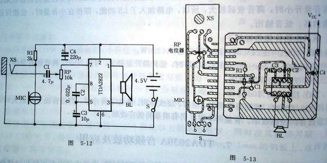
喊话器、功率接续器(有源音箱)两用机电原理图如图5-12所示,本电路即可作小型扩音喊话使用,也可适用于袖珍立体收放机、收音
机,作为音频功率放大器用扬声器放音。整个电路采用3节5号电池(4.5)供电,其静态电流为6mA ~ 9mA,输出功率可达1W左右。
本电路将TDA2822集成内部的两个功放级接成桥式电路,称BTL电路。BTL电路的优点是:制作容易,携带使用方便,可减少失真, 改善音质,增加输出功率,并使电路大为简化。
【电路原理】
本机工作原理如下:合上开关S,当对面话筒MIC讲话时,音频话音就经C1、RP从集成电路TDA2822的⑦脚输入,经过内部BTL功放电路
放大后,由扬声器BL发生时,发音清晰明亮,并可由电位器RP调节音量的大小。
【制作方法】
先按电路图清点并选择下列元件:
(1) 集成电路TDA2822:1只;
(2) 8脚插座:1只;
(3) 电解电容器:C4 220μF/10V 1只;C2、C3 10μF/6.3V 2只;C1 4.7μF/6.3V 1只;
(4) 电位器RP:10kΩ 1只;
(5) 电阻器R:3kΩ 1只;
(6) 电源开关S:(1 X 1)拨动开关 1只;
(7) 驻极体电容话筒:1只;
(8) 2英寸扬声器:1只;
(9) 透明塑料机壳:1只;
(10) 印制电路板:2cm X 8cm 1块; 5.5cm X 5.2cm 1块;
(11) 立体声三芯插头:Φ3mm 1只;
(12) 金属屏蔽线:1根。
按图5-12将上述各元件焊接在印刷电路板上,如图5-13所示。制作时先将开关S、话筒MIC、集成电路TDA2822、扬声器BL固定后焊接在
印刷板上,然后对照图5-12电路将R1、C1 ~ C4连接线焊在印刷板上。
对照电路、焊接元件无误后,开始接上电源,进行调试、检查。因电路外围元件少,本机无须调试就能成功。
第二篇:TDA2822
查询TDA2822供应商
TDA2822
....DUALPOWERAMPLIFIERSUPPLYVOLTAGEDOWNTO3VLOWCROSSOVERDISTORSION
LOWQUIESCENTCURRENT
BRIDGEORSTEREOCONFIGURATION
POWERDIP
(Plastic12+2+2)
ORDERINGNUMBER:TDA2822DESCRIPTION
TheTDA2822isamonolithicintegratedcircuitin12+2+2powerdip,intendedforuseasdualaudiopoweramplifierinportableradiosandTSsets.TYPICALAPPLICATIONCIRCUIT(STEREO)March19951/11
TDA2822
PINCONNECTION(topview)
SCHEMATICDIAGRAM
ABSOLUTEMAXIMUMRATINGS
SymbolVsIoPtotTstg,Tj
SupplyVoltageOutputPeakCurrent
TotalPowerDissipationatTamb=50°CatTcase=70°C
StorageandJunctionTemperature
Parameter
Value151.51.254–40to150
UnitVAWW°C
2/11
TDA2822

THERMALDATA
SymbolRthj-ambRthj-case
Parameter
ThermalResistanceJunction-ambientThermalResistanceJunction-pins
MaxMax
Value8020
Unit°C/W°C/W
ELECTRICALCHARACTERISTICS(Vs=6V,Tamb=25°C,unlessotherwisespecified)STEREO(testcircuitoffig.1)
SymbolVsVcIdIbPo
Parameter
SupplyVoltage
QuiescentOutputVoltageQuiescentDrainCurrentInputBiasCurrentOutputPower(eachchannel)
d=10%Vs=9VVs=6VVs=4.5Vf=1kHzf=1kHz
Rs=10k?
B=22Hzto22kHzCurveAf=100Hz
Rg=10k?f=1kHz
24
f=1kHzRL=4?RL=4?RL=4?
1.30.4536100
2.523050
Vs=9VVs=6V
TestCondition
Min.3
42.761001.70.650.3239
4112
Typ.
Max.15
UnitVVVmAnAWWWdBk?μVμVdBdB
GvRi
e
ClosedLoopVoltageGainInputResistanceTotalInputNoise
N
SVRCS
SupplyVoltageRejectionChannelSeparation
BRIDGE(testcircuitoffig.2)
VsIdVosIbPo
SupplyVoltage
QuiescentDrainCurrentOutputOffsetVoltageInputBiasCurrentOutputPower
d=10%f=1kHzVs=9VRL=8?Vs=6VRL=8?Vs=4.5VRL=4?RL=8?f=1kHzf=1kHz
Rs=10k?
B=22Hzto22kHzCurveAf=100Hz
100
32.540
Po=0.5W
2.70.9
RL=∞RL=8?
3
6101003.21.3510.239
151260
VmAmVnAWWW%dBk?μVμVdB
dGvRi
e
Distortion(f=1kHz)ClosedLoopVoltageGainInputResistanceTotalInputNoise
N
SVRSupplyVoltageRejection
3/11
TDA2822Figure1:TestCircuit(stereo).
Figure2:P.C.BoardandComponentsLayoutoftheCircuitofFigure1(1:1scale).4/11
TDA2822

Figure3:TestCircuit(bridge).
Figure4:P.C.BoardandComponentsLayoutoftheCircuitofFigure3(1:1scale).
5/11
TDA2822Figure5:OutputPowervs.SupplyVoltage
(Stereo).Figure6:OutputPowervs.SupplyVoltage(Bridge).
Figure7:Distorsionvs.OutputPower(Bridge).Figure8:Distorsionvs.OutputPower(Bridge).Figure9:SupplyVoltageRejectionvs.
Frequency.Figure10:QuiescentCurrentvs.SupplyVoltage.
6/11
TDA2822
Figure11:TotalPowerDissipationvs.Output
Power(Stereo).Figure12:TotalPowerDissipationvs.OutputPower(Bridge).
Figure13:TotalPowerDissipationvs.Output
Power(Bridge).
7/11
TDA2822Figure14:ApplicationCircuitforPortableRadios.MOUNTINGINSTRUCTION
TheRthj-amboftheTDA2822canbereducedbysol-deringtheGNDpinstoasuitablecopperareaoftheprintedcircuitboard(Figure15)ortoanexternalheatsink(Figure16).
ThediagramofFigure17showsthemaximumdis-sipablepowerPtotandtheRthj-ambasafunctionoftheside”?”oftwoequalsquarecopperareashavingathicknessof35μ(1.4mils).
Figure15:ExampleofP.C.BoardCopperArea
whichisusedasHeatsink.Duringsolderingthepinstemperaturemustnotex-ceed260°Candthesolderingtimemustnotbelongerthan12seconds.Theexternalheatsinkorprintedcircuitcopperareamustbeconnectedtoelectricalground.Figure16:ExternalHeatsinkMountingExample.
8/11
TDA2822

Figure6:MaximumDissipablePowerand
JunctiontoAmbientThermal
Resistancevs.Side”?”.Figure7:MaximumAllowablePowerDissipationvs.AmbientTemperature.
9/11
TDA2822
POWERDIP16PACKAGEMECHANICALDATA
DIM.
MIN.
a1Bbb1DEee3FILZ
3.30
1.27
8.802.5417.78
7.105.10
0.130
0.050
0.380.510.85
0.50
0.5020.0
0.3460.1000.700
0.2800.201
0.015
1.40
mmTYP.
MAX.
MIN.0.0200.033
0.020
0.0200.7870.055
inchTYP.
MAX.
10/11
TDA2822

Informationfurnishedisbelievedtobeaccurateandreliable.However,SGS-THOMSONMicroelectronicsassumesnoresponsibilityfortheconsequencesofuseofsuchinformationnorforanyinfringementofpatentsorotherrightsofthirdpartieswhichmayresultfromitsuse.NolicenseisgrantedbyimplicationorotherwiseunderanypatentorpatentrightsofSGS-THOMSONMicroelectronics.Specifica-tionsmentionedinthispublicationaresubjecttochangewithoutnotice.Thispublicationsupersedesandreplacesallinformationpre-viouslysupplied.SGS-THOMSONMicroelectronicsproductsarenotauthorizedforuseascriticalcomponentsinlifesupportdevicesorsystemswithoutexpresswrittenapprovalofSGS-THOMSONMicroelectronics.
?1995SGS-THOMSONMicroelectronics-AllRightsReserved
SGS-THOMSONMicroelectronicsGROUPOFCOMPANIES
Australia-Brazil-France-Germany-HongKong-Italy-Japan-Korea-Malaysia-Malta-Morocco-TheNetherlands-Singapore-
Spain-Sweden-Switzerland-Taiwan-Thaliand-UnitedKingdom-U.S.A.
11/11